PCK2000M View Datasheet(PDF) - Philips Electronics
Part Name
Description
Manufacturer
PCK2000M Datasheet PDF : 12 Pages
| |||
Philips Semiconductors
CK97 (66/100MHz) Mobile System Clock Generator
Product specification
PCK2000M
PIN DESCRIPTION
PIN NUMBER
SYMBOL
FUNCTION
26
REF
14.318 MHz clock output
28
VSSREF
GROUND for REF output
27
VDDREF
POWER for REF output
1
XTAL_IN
14.318 MHz crystal input
2
XTAL_OUT
14.318 MHz crystal output
3, 12
4
VSSPCI [0–1]
PCICLK_F
GROUND for PCI outputs
Free-running PCI output
6, 9
5, 7, 8, 10, 11
VDDPCI [0–1]
PCICLK [1–5]
POWER for PCI outputs
PCI clock outputs.
13, 21
14, 20
16
VDDCORE [0–1]
VSSCORE [0–1]
SEL
Isolated POWER for core
Isolated GROUND for core
Logic select pins
15
SEL100/66
Select pin for enabling 66 MHz or 100MHz or 66 MHz. L = 66 Mhz
H = 100MHz
17
PWRDWN
Control pin to put device in powerdown state, active low
18
CPUSTOP
Control pin to disable CPU clocks, active low
19
PCISTOP
Control pin to disable PCI clocks, active low
25
22
23, 24
VDDCPU
VSSCPU
CPUCLK [0–1]
Power for CPU outputs
GROUND for CPU outputs
CPU and Host clock outputs 2.5V
NOTE:
1. VDD and VSS names in the above tables reflects a likely internal POWER and GROUND partition to reduce the effects of internal noise on
the performance of the device. In reality, the platform will be configured with the VDDCPU pins tied to a 2.5V supply, all remaining VDD pins
tied to a common 3.3V supply and all VSS pins being common.
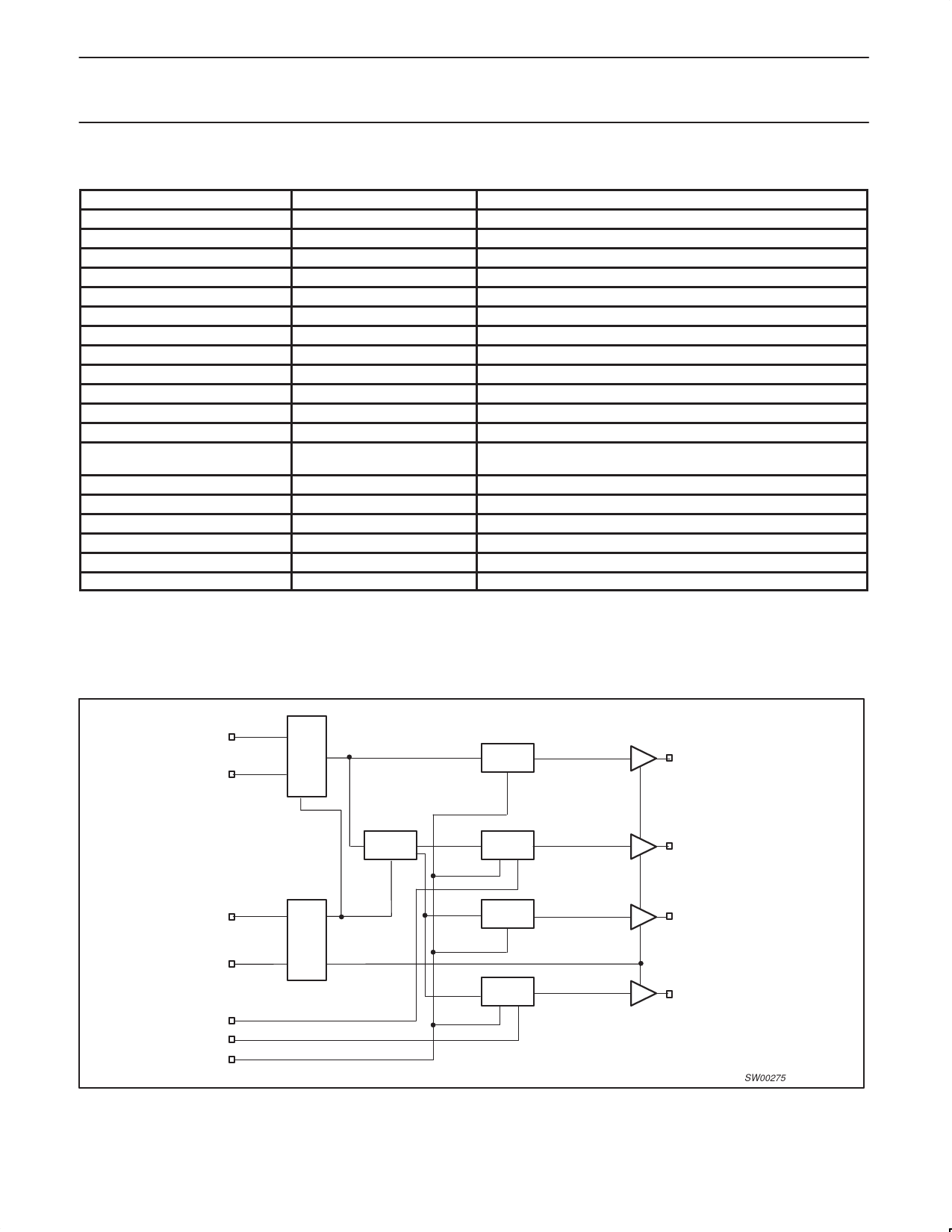
BLOCK DIAGRAM
XTAL_IN X
XTAL_OUT X
14.318
MHZ
OSC
PWRDWN
LOGIC
X REFCLK (14.318 MHz)
PLL1
SEL0 X
SEL100/66 X
CPUSTOP X
PCISTOP X
PWRDWN X
LOGIC
STOP
LOGIC
PWRDWN
LOGIC
STOP
LOGIC
X CPUCLK [0–1]
X PCICLK_F (33MHz)
X PCICLK [1–5] (33MHz)
SW00275
1998 Sep 29
3
Share Link: 