PSD913G3-C-90JI View Datasheet(PDF) - STMicroelectronics
Part Name
Description
Manufacturer
PSD913G3-C-90JI Datasheet PDF : 94 Pages
| |||
Preliminary Information
PSD9XX Family
PSD9XX
Architectural
Overview
(cont.)
5.4 I/O Ports
The PSD9XX has 27 I/O pins divided among four ports (Port A, B, C, and D). Each
I/O pin can be individually configured for different functions. Ports A, B, C and D can
be configured as standard MCU I/O ports, PLD I/O, or latched address outputs for
microcontrollers using multiplexed address/data busses.
The JTAG pins can be enabled on Port C for In-System Programming (ISP).
Port A can also be configured as a data port for a non-multiplexed bus.
5.5 Microcontroller Bus Interface
The PSD9XX easily interfaces with most 8-bit microcontrollers that have either
multiplexed or non-multiplexed address/data busses. The device is configured to respond
to the microcontroller’s control signals, which are also used as inputs to the PLDs. Section
9.3.5 contains microcontroller interface examples.
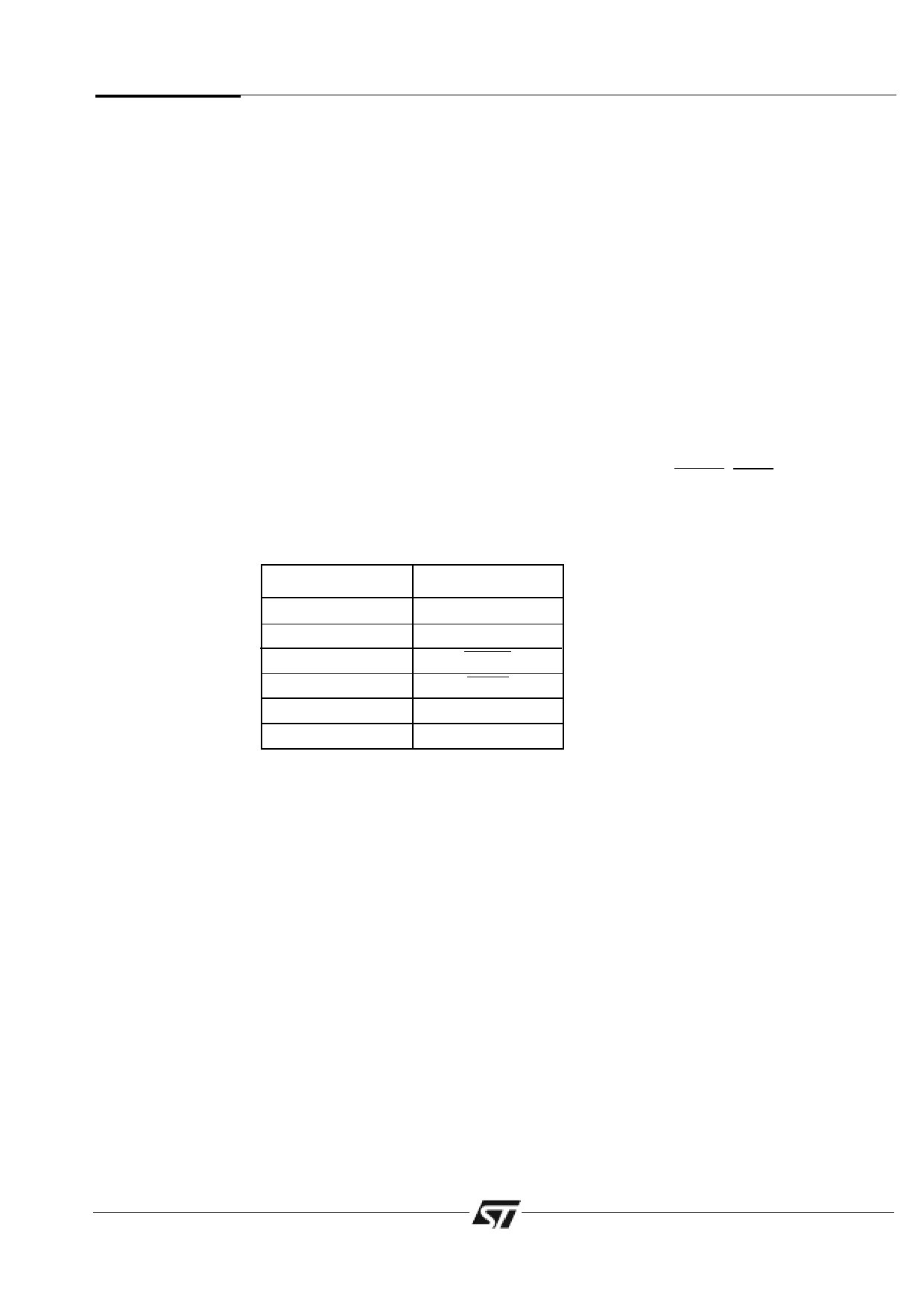
5.6 JTAG Port
In-System Programming can be performed through the JTAG pins on Port C. This serial
interface allows complete programming of the entire PSD9XX device. A blank device can
be completely programmed. The JTAG signals (TMS, TCK, TSTAT, TERR, TDI, TDO) are
enabled on Port C when selected or when a device is blank. Table 3 indicates the JTAG
signals pin assignments.
Table 3. JTAG Signals on Port C
Port C Pins
JTAG Signal
PC0
TMS
PC1
TCK
PC3
TSTAT
PC4
TERR
PC5
TDI
PC6
TDO
7
Share Link: 