TC642B View Datasheet(PDF) - Microchip Technology
Part Name
Description
Manufacturer
TC642B Datasheet PDF : 36 Pages
| |||
TC642B/TC647B
3.0 PIN FUNCTIONS
The description of the pins are given in Table 3-1.
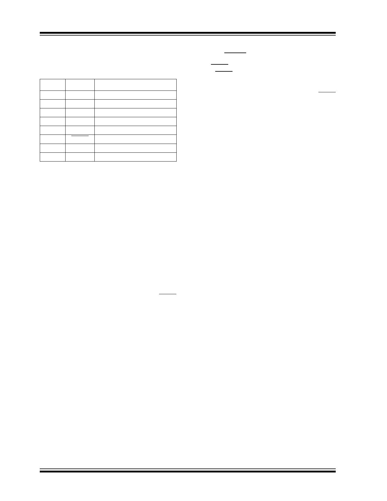
TABLE 3-1: PIN FUNCTION TABLE
Pin
Name
Function
1
VIN Analog Input
2
CF Analog Output
3
VMIN Analog Input
4
GND Ground
5
SENSE Analog Input
6
FAULT Digital (Open-Drain) Output
7
VOUT Digital Output
8
VDD Power Supply Input
3.1 Analog Input (VIN)
The thermistor network (or other temperature sensor)
connects to VIN. A voltage range of 1.20V to 2.60V (typ-
ical) on this pin drives an active duty cycle of 0% to
100% on the VOUT pin.
3.2 Analog Output (CF)
CF is the positive terminal for the PWM ramp generator
timing capacitor. The recommended value for the CF
capacitor is 1.0 µF for 30 Hz PWM operation.
3.3 Analog Input (VMIN)
An external resistor divider connected to VMIN sets the
minimum fan speed by fixing the minimum PWM duty
cycle (1.20V to 2.60V = 0% to 100%, typical). The
TC642B and TC647B devices enter shutdown mode
when 0 VMIN VSHDN. During shutdown, the FAULT
output is inactive and supply current falls to 30 µA
(typical).
3.4 Analog Input (SENSE)
Pulses are detected at SENSE as fan rotation chops
the current through a sense resistor. The absence of
pulses indicates a fan fault condition.
3.5 Digital (Open-Drain) Output
(FAULT)
The FAULT line goes low to indicate a fault condition.
When FAULT goes low due to a fan fault, the output will
remain low until the fan fault condition has been
removed (16 pulses have been detected at the SENSE
pin in a 32/f period). For the TC642B device, the FAULT
output will also be asserted when the VIN voltage
reaches the VOTF treshold of 2.62V (typical). This gives
an over-temperature/100% fan speed indication.
3.6 Digital Output (VOUT)
VOUT is an active-high complimentary output and
drives the base of an external NPN transistor (via an
appropriate base resistor) or the gate of an N-channel
MOSFET. This output has asymmetrical drive. During a
fan fault condition, the VOUT output is continuously on.
3.7 Power Supply Input (VDD)
The VDD pin with respect to GND provides power to the
device. This bias supply voltage may be independent of
the fan power supply.
DS21756C-page 10
2002-2013 Microchip Technology Inc.
Share Link: 