TC642B View Datasheet(PDF) - Microchip Technology
Part Name
Description
Manufacturer
TC642B Datasheet PDF : 36 Pages
| |||
TC642B/TC647B
1.0 ELECTRICAL
CHARACTERISTICS
Absolute Maximum Ratings †
Supply Voltage (VDD) .......................................................6.0V
Input Voltage, Any Pin................(GND - 0.3V) to (VDD +0.3V)
Operating Temperature Range ....................- 40°C to +125°C
Maximum Junction Temperature, TJ ........................... +150°C
ESD Protection on all pins ........................................... > 3 kV
† Notice: Stresses above those listed under “Maximum
Ratings” may cause permanent damage to the device. This is
a stress rating only and functional operation of the device at
those or any other conditions above those indicated in the
operational listings of this specification is not implied. Expo-
sure to maximum rating conditions for extended periods may
affect device reliability.
ELECTRICAL SPECIFICATIONS
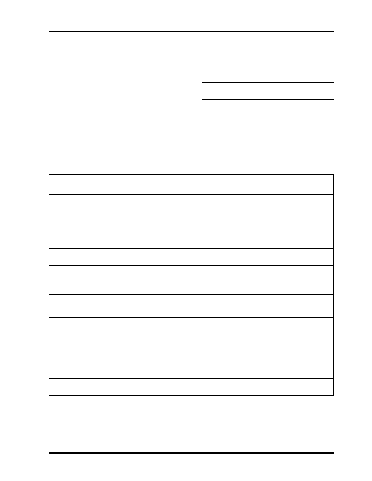
PIN FUNCTION TABLE
Name
VIN
CF
VMIN
GND
SENSE
FAULT
VOUT
VDD
Function
Analog Input
Analog Output
Analog Input
Ground
Analog Input
Digital (Open-Drain) Output
Digital Output
Power Supply Input
Electrical Specifications: Unless otherwise specified, all limits are specified for -40°C < TA < +85°C, VDD = 3.0V to 5.5V.
Parameters
Sym
Min
Typ
Max
Units
Conditions
Supply Voltage
Supply Current, Operating
VDD
3.0
—
5.5
IDD
—
200
400
Supply Current, Shutdown Mode
IDD(SHDN)
—
30
—
VOUT Output
Sink Current at VOUT Output
Source Current at VOUT Output
VIN, VMIN Inputs
Input Voltage at VIN or VMIN for 100%
PWM Duty Cycle
IOL
IOH
VC(MAX)
1.0
5.0
2.45
—
—
2.60
Over-Temperature Indication
Threshold
VOTF
VC(MAX) +
20 mV
Over-Temperature Indication
VOTF-HYS
80
Threshold Hysteresis
VC(MAX) - VC(MIN)
Minimum Speed Threshold
Voltage Applied to VMIN to Ensure
Shutdown Mode
VC(SPAN)
1.3
1.4
VMIN
VC(MAX) -
VC(SPAN)
VSHDN
—
—
Voltage Applied to VMIN to Release
Shutdown Mode
VREL
VDD x 0.19
—
Hysteresis on VSHDN, VREL
VIN, VMIN Input Leakage
Pulse-Width Modulator
VHYST
IIN
—
- 1.0
0.03 x VDD
—
PWM Frequency
fPWM
26
30
Note 1: Ensured by design, tested during characterization.
2: For VDD < 3.7V, tSTARTUP and tMP timers are typically 13/f.
—
—
2.75
1.5
VC(MAX)
VDD x 0.13
—
—
+1.0
34
V
µA Pins 6, 7 Open,
CF = 1 µF, VIN = VC(MAX)
µA Pins 6, 7 Open,
CF = 1 µF, VMIN = 0.35V
mA VOL = 10% of VDD
mA VOH = 80% of VDD
V
V For TC642B Only
mV For TC642B Only
V
V
V
V VDD = 5V
V
µA Note 1
Hz CF = 1.0 µF
2002-2013 Microchip Technology Inc.
DS21756C-page 3
Share Link: 