80C196NT View Datasheet(PDF) - Intel
Part Name
Description
Manufacturer
80C196NT Datasheet PDF : 31 Pages
| |||
8XC196NT
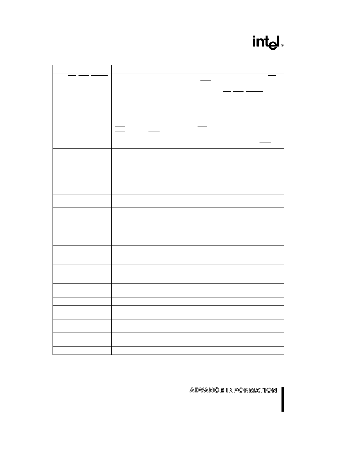
PIN DESCRIPTIONS (Continued)
Symbol
Name and Function
P5 2 WR WRL SLPWR
Write and Write Low output to external memory as selected by the CCR WR
will go low for every external write while WRL will go low only for external
writes where an even byte is being written WR WRL is active during external
memory writes Also an LSIO pin when not used as WR WRL SLPWR is the
Slave Port Write Control Input
P5 5 BHE WRH
Byte High Enable or Write High output as selected by the CCR BHEe0
selects the bank of memory that is connected to the high byte of the data bus
A0e0 selects that bank of memory that is connected to the low byte Thus
accesses to a 16-bit wide memory can be to the low byte only (A0e0
BHEe1) to the high byte only (A0e1 BHEe0) or both bytes (A0e0
BHEe0) If the WRH function is selected the pin will go low if the bus cycle is
writing to an odd memory location BHE WRH is only valid during 16-bit
external memory read write cycles Also an LSIO pin when not BHE WRH
P5 6 READY
Ready input to lengthen external memory cycles for interfacing with slow or
dynamic memory or for bus sharing If the pin is high CPU operation continues
in a normal manner If the pin is low prior to the falling edge of CLKOUT the
memory controller goes into a wait state mode until the next positive transition
in CLKOUT occurs with READY high When external memory is not used
READY has no effect The max number of wait states inserted into the bus
cycle is controlled by the CCR CCR1 Also an LSIO pin when READY is not
selected
P5 4 SLPINT
Dual function I O pin As a bidirectional port pin or as a system function The
system function is a Slave Port Interrupt Output Pin
P6 2 T1CLK
Dual function I O pin Primary function is that of a bidirectional I O pin
however it may also be used as a TIMER1 Clock input The TIMER1 will
increment or decrement on both positive and negative edges of this pin
P6 3 T1DIR
Dual function I O pin Primary function is that of a bidirectional I O pin
however it may also be used as a TIMER1 Direction input The TIMER1 will
increment when this pin is high and decrements when this pin is low
PORT1 EPA0–7
P6 0–6 1 EPA8–9
Dual function I O port pins Primary function is that of bidirectional I O System
function is that of High Speed capture and compare EPA0 and EPA2 have yet
another function of T2CLK and T2DIR of the TIMER2 timer counter
PORT 0 ACH4–7
4-bit high impedance input-only port These pins can be used as digital inputs
and or as analog inputs to the on-chip A D converter These pins are also
used as inputs to OTPROM parts to select the Programming Mode
P6 3–6 7 SSIO
Dual function I O ports that have a system function as Synchronous Serial I O
Two pins are clocks and two pins are data providing full duplex capability
PORT 2
8-bit multi-functional port All of its pins are shared with other functions
PORT 3 and 4
8-bit bidirectional I O ports with open drain outputs These pins are shared
with the multiplexed address data bus which has strong internal pullups
EPORT
8-bit bidirectional standard and I O port These bits are shared with the
extended address bus A16 – A19 Pin function is selected on a per pin basis
INTOUT
Interrupt Output This active-low output indicates that a pending interrupt
requires use of the external bus
SLP0 – SLP7
Slave Port Address Data Bus
6
Share Link: 