TDA8922 View Datasheet(PDF) - Philips Electronics
Part Name
Description
Manufacturer
TDA8922 Datasheet PDF : 36 Pages
| |||
Philips Semiconductors
2 ├Ś 25 W class-D power ampli’¼üer
Objective speci’¼ücation
TDA8922
16 APPLICATION INFORMATION
16.1 BTL application
When using the power amplifier in a mono BTL application
(for more output power), the inputs of both channels must
be connected in parallel and the phase of one of the inputs
must be inverted (see Fig.6). In principle the loudspeaker
can be connected between the outputs of the two
single-ended demodulation filters.
16.2 Pin MODE
For correct operation the switching voltage at pin MODE
should be debounced. If pin MODE is driven by a
mechanical switch an appropriate debouncing low-pass
filter should be used. If pin MODE is driven by an
electronic circuit or microcontroller then it should remain at
the mute voltage level for at least 100 ms before switching
back to the standby voltage level.
16.3 Output power estimation
The output power in several applications (SE and BTL)
can be estimated using the following expressions:
SE: Po(1%) = ---R----------L------R--+------L----0------.----6-------├Ś-----V----P-2---├Ś--├Ś---(--R-1----L-ŌĆō----t--m----i-n----├Ś-----f--o---s---c--)-----2-
Maximum current:
Io(peak) = -V----P----├Ś-----(--R-1----LŌĆō----+-t--m--0--i-.n--6--├Ś-----f--o---s--c----) should not exceed 4 A.
BTL: Po(1%) = ----R---------L------R--+------L----1------.----2-------├Ś-----2---V----2-P----├Ś├Ś-----R(--1--L---ŌĆō-----t--m----i-n----├Ś-----f--o---s--c---)-----2-
Maximum current:
Io(peak) = -2---V-----P----├Ś-----(R--1---L--ŌĆō--+---t--m1---.-i-2n----├Ś-----f--o---s--c---) should not exceed 4 A.
Legend:
RL = load impedance
fosc = oscillator frequency
tmin = minimum pulse width (typical 190 ns)
VP = single-sided supply voltage (so, if supply is ┬▒30 V
symmetrical, then VP = 30 V)
Po(1%) = output power just at clipping
Po(10%) = output power at THD = 10%
Po(10%) = 1.25 ├Ś Po(1%).
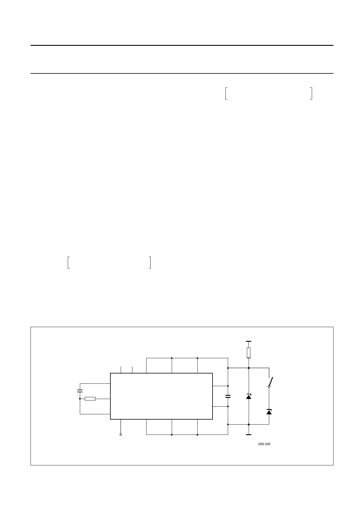
16.4 External clock
The minimum required symmetrical supply voltage for
external clock application is ┬▒15 V (equally, the minimum
asymmetrical supply voltage for applications with an
external clock is 30 V).
When using an external clock the following accuracy of the
duty cycle of the external clock has to be taken into
account: 47.5% < ╬┤ < 52.5%.
A possible solution for an external clock oscillator circuit is
illustrated in Fig.8.
handbook, full pagewidth
VDDA
2 kŌä”
0ŌłÆ 0+
11 10
CTC 1
120 pF
RTC 2
9.1 kŌä”
RCTC 3 13
ASTABŌłÆ
4
ASTAB+
5
ŌłÆTRIGGER
6
14 VDD
HEF4047BT
7 VSS
8
9
+TRIGGER MR
12
RETRIGGER
360 kHz 320 kHz
220
nF
5.6 V
HOP
4.3 V
CLOCK
Fig.8 External oscillator circuit.
GND
MBL468
2003 Mar 20
16
Share Link: 