TS2012IQT View Datasheet(PDF) - STMicroelectronics
Part Name
Description
Manufacturer
TS2012IQT Datasheet PDF : 30 Pages
| |||
Application information
4
Application information
TS2012
4.1
Differential configuration principle
The TS2012 is a monolithic fully-differential input/output class D power amplifier. The
TS2012 also includes a common-mode feedback loop that controls the output bias value to
average it at VCC/2 for any DC common mode input voltage. This allows the device to
always have a maximum output voltage swing, and by consequence, maximize the output
power. Moreover, as the load is connected differentially compared with a single-ended
topology, the output is four times higher for the same power supply voltage.
The advantages of a full-differential amplifier are:
● High PSRR (power supply rejection ratio)
● High common mode noise rejection
● Virtually zero pop without additional circuitry, giving a faster start-up time compared
with conventional single-ended input amplifiers
● Easier interfacing with differential output audio DAC
● No input coupling capacitors required thanks to common mode feedback loop
4.2
Note:
Gain settings
In the flat region of the frequency-response curve (no input coupling capacitor or internal
feedback loop + load effect), the differential gain can be set to 6, 12 18, 24 dB depending on
the logic level of the G0 and G1 pins, as shown in Table 9.
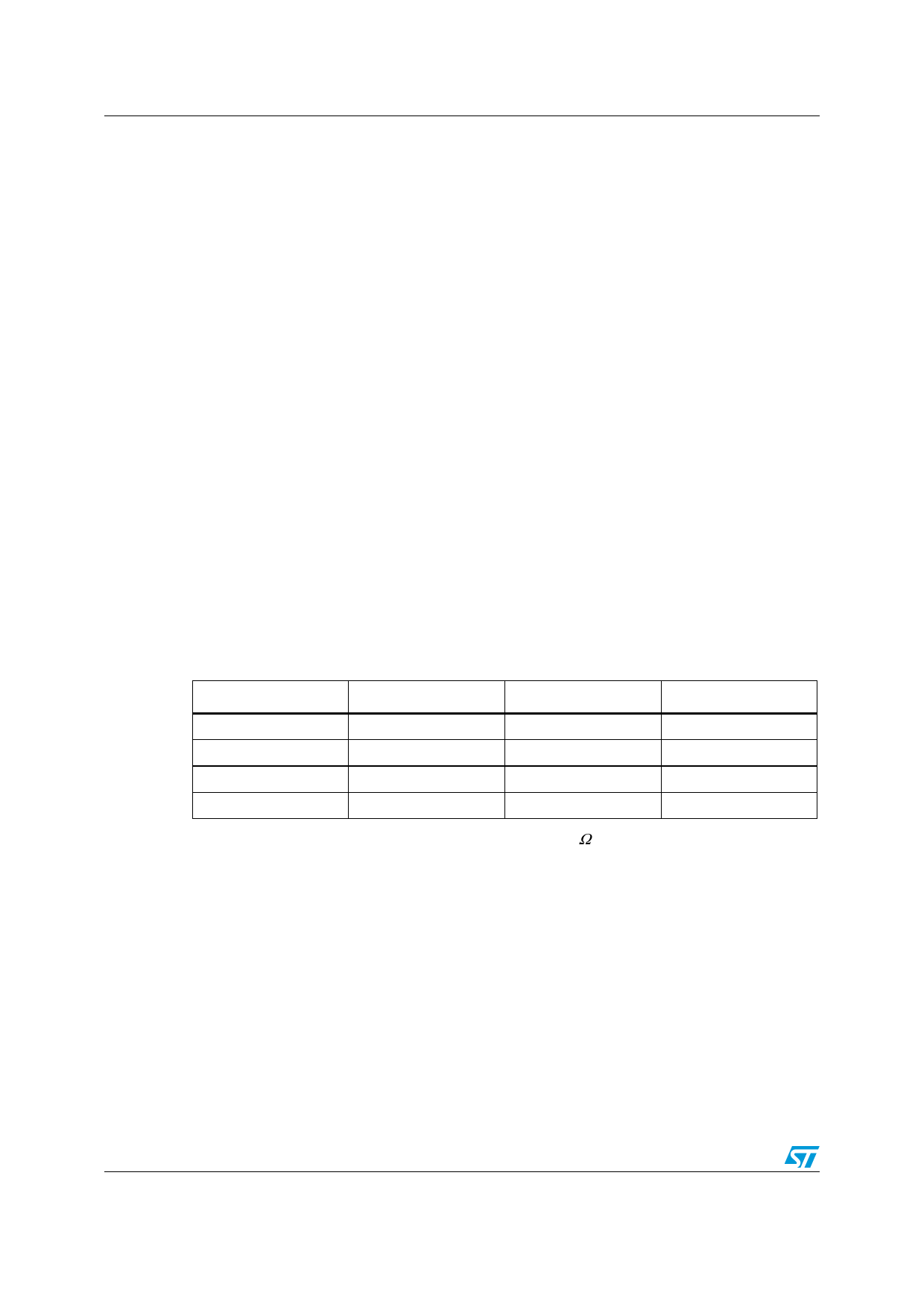
Table 9. Gain settings with G0 and G1 pins
G1
G0
Gain (dB)
Gain (V/V)
0
0
6
2
0
1
12
4
1
0
18
8
1
1
24
16
Between pins G0, G1 and GND there is an internal 300kΩ (+/-20%) resistor. When the pins
are floating, the gain is 6 dB. In full standby (left and right channels OFF), these resistors are
disconnected (HiZ input).
4.3
Common mode feedback loop limitations
As explained previously, the common mode feedback loop allows the output DC bias voltage
to be averaged at VCC/2 for any DC common mode bias input voltage.
Due to the Vic limitation of the input stage (see Table 2: Operating conditions on page 4), the
common mode feedback loop can fulfil its role only within the defined range.
22/30
Share Link: 