UPD17P401CG-XXX-3B9 View Datasheet(PDF) - NEC => Renesas Technology
Part Name
Description
Manufacturer
UPD17P401CG-XXX-3B9
NEC => Renesas Technology

UPD17P401CG-XXX-3B9 Datasheet PDF : 32 Pages
| |||
µPD17P401
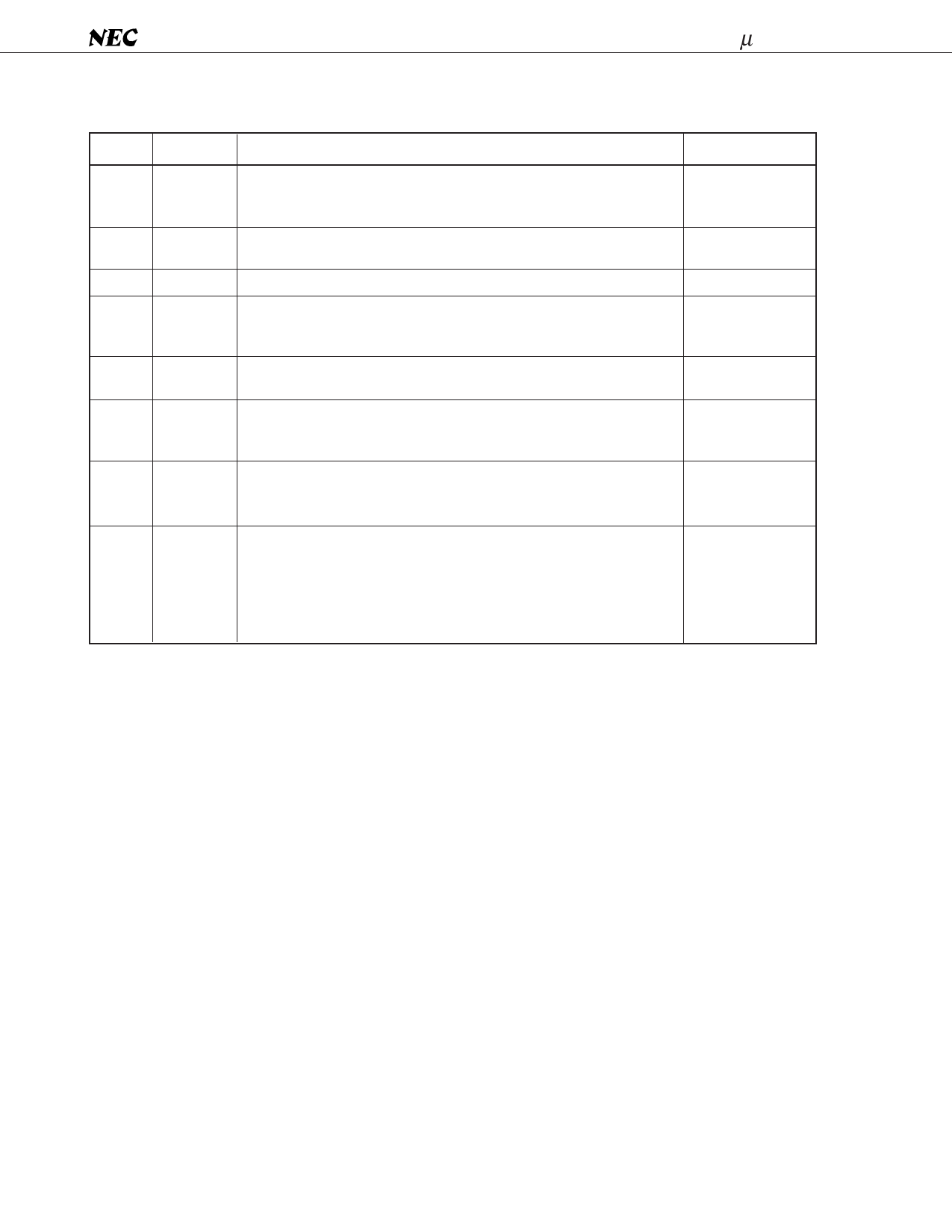
1.2 PROM PROGRAMMING MODE
PIN NO.
33
36
37
48
50
53
58
|
61
62
|
65
66
|
69
SYMBOL
GND
VDD1
CLK
VPP
VDD2
GND
FUNCTION
Ground.
Pins 33 and 53 are connected within the chip, but should also be
connected to the same potential externally.
Positive power supply. Applies 6 V in grogram memory write, read
and verify operations.
PROM programming clock input.
Positive power supply for PROM programming.
Applies 12.5 V as program voltage in program memory write, read and
verify operations.
Positive power supply. Applies 6 V in program memory write, read
and verify operations.
Ground.
Pins 33 and 53 are connected within the chip, but should also be
connected to the same potential externally.
OUTPUT TYPE
—
—
—
—
—
—
MD3
|
MD0
D3
|
D0
D7
|
D4
Operating mode selection inputs for PROM programming.
PROM programming 8-bit data input/output.
—
CMOS push-pull
Remarks Pins other than the above are not used in the PROM programming mode. See “PIN CONFIGU-
RATION (2) PROM PROGRAMMING MODE” for the disposition of unused pins.
10
Share Link: