UPD75238GJ View Datasheet(PDF) - NEC => Renesas Technology
Part Name
Description
Manufacturer
UPD75238GJ Datasheet PDF : 190 Pages
| |||

µPD75238
2.2 GENERAL REGISTER BANK CONFIGURATION
The µPD75238 contains four register banks, each consisting of eight general registers: X, A, B, C, D, E, H,
and L. These registers are mapped to addresses 00H to 1FH in memory bank 0 of the data memory. (See Fig.
2-2.) To specify a general register bank, a register bank enable flag (RBE) and a register bank select register
(RBS) are contained. The RBS is a register used to select a register bank, and the RBE is a flag used to determine
whether a register bank selected using the RBS is to be enabled. The register bank (RB) enabled at instruction
execution is determined as RB = RBE• RBS
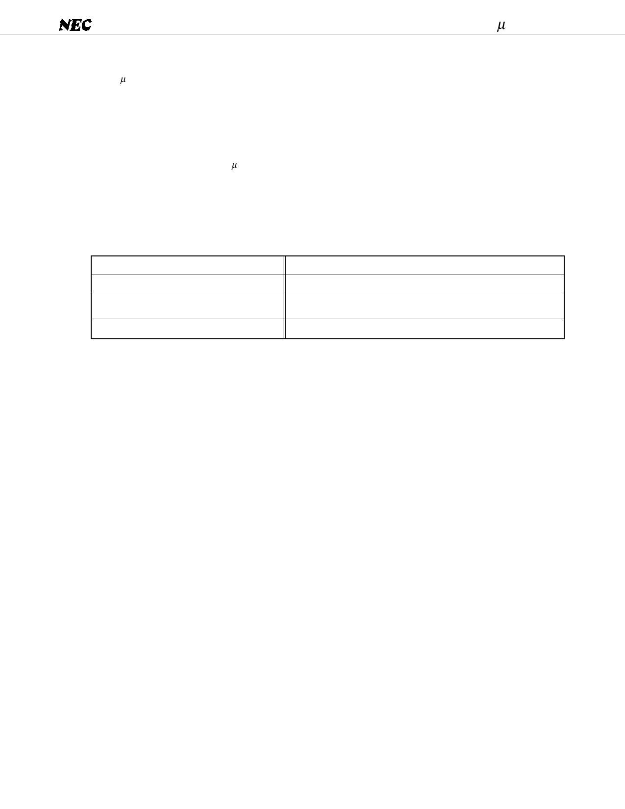
As indicated in Table 2-2, the µPD75238 enables the user to create programs in a very efficient manner by
selecting a register bank from the four register banks, depending on whether the processing is normal
processing or interrupt processing. (The RBE is automatically saved and set at the time of interrupt processing,
and is automatically restored upon completion of interrupt processing.)
Table 2-2 Recommended Use of Register Banks with Normal Routines and Interrupt Routines
Normal processing
Use register banks 2 and 3 with RBE = 1.
Single interrupt processing
Use register bank 0 with RBE = 0.
Dual interrupt processing
Use register bank 1 with RBE = 1.
(In this case, the RBS needs to be saved and restored.)
Multiple (triple or more) interrupt processing Save and restore the registers with PUSH or POP.
The general registers allow transfers, comparisons, arithmetic/logical operations, and increments and
decrements not only on a 4-bit basis, but also on an 8-bit basis with the XA, HL, DE, and BC register pairs.
In this case, the register pairs of the register bank that has the inverted value of bit 0 of a register bank specified
by RBE• RBS can be specified as XA’, HL’, DE’, and BC’, thus providing eight 8-bit registers. (See Fig. 2-3.)
19