UPD784936A View Datasheet(PDF) - NEC => Renesas Technology
Part Name
Description
Manufacturer
UPD784936A Datasheet PDF : 102 Pages
| |||
µPD784935A,784936A,784937A,784938A
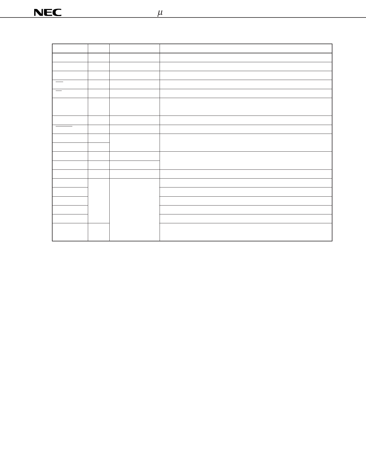
6.2 Non-Port Pins (2/2)
Pin Name
CLKOUT
PWM0
PWM1
RX
TX
REGC
I/O
Output
Output
Output
Input
Output
—
Alternate Function
ASTB
—
—
—
—
—
REGOFF
RESET
X1
X2
XT1
XT2
ANI0 to ANI7
AVREF1
AVDD
AVSS
VDD
VSS
IC
—
Input
Input
—
Input
—
Input
—
Input
—
—
—
—
—
P70 to P77
—
Function
Clock output
PWM output 0
PWM output 1
Data input (IEBus)
Data output (IEBus)
Capacitor connection for regulation output stabilization/power supply when
regulator is stopped
Regulator operation specification signal
Chip reset
Crystal connection for system clock oscillation (clock can be also input to X1.)
Watch clock connection
Analog voltage input for A/D converter
Application of reference voltage for A/D converter
Positive power supply for A/D converter
GND for A/D converter
Positive power supply
GND
Internally connected. Connect this pin directly to VSS (this pin is used to test
the IC.)
Data Sheet U13572EJ2V0DS
17
Share Link: 