DSP16410C View Datasheet(PDF) - Agere -> LSI Corporation
Part Name
Description
Manufacturer
DSP16410C Datasheet PDF : 373 Pages
| |||
DSP16410C Digital Signal Processor
Data Addendum
May 2001
5 Ball Grid Array Information (continued)
5.1 208-Ball PBGA Package (continued)
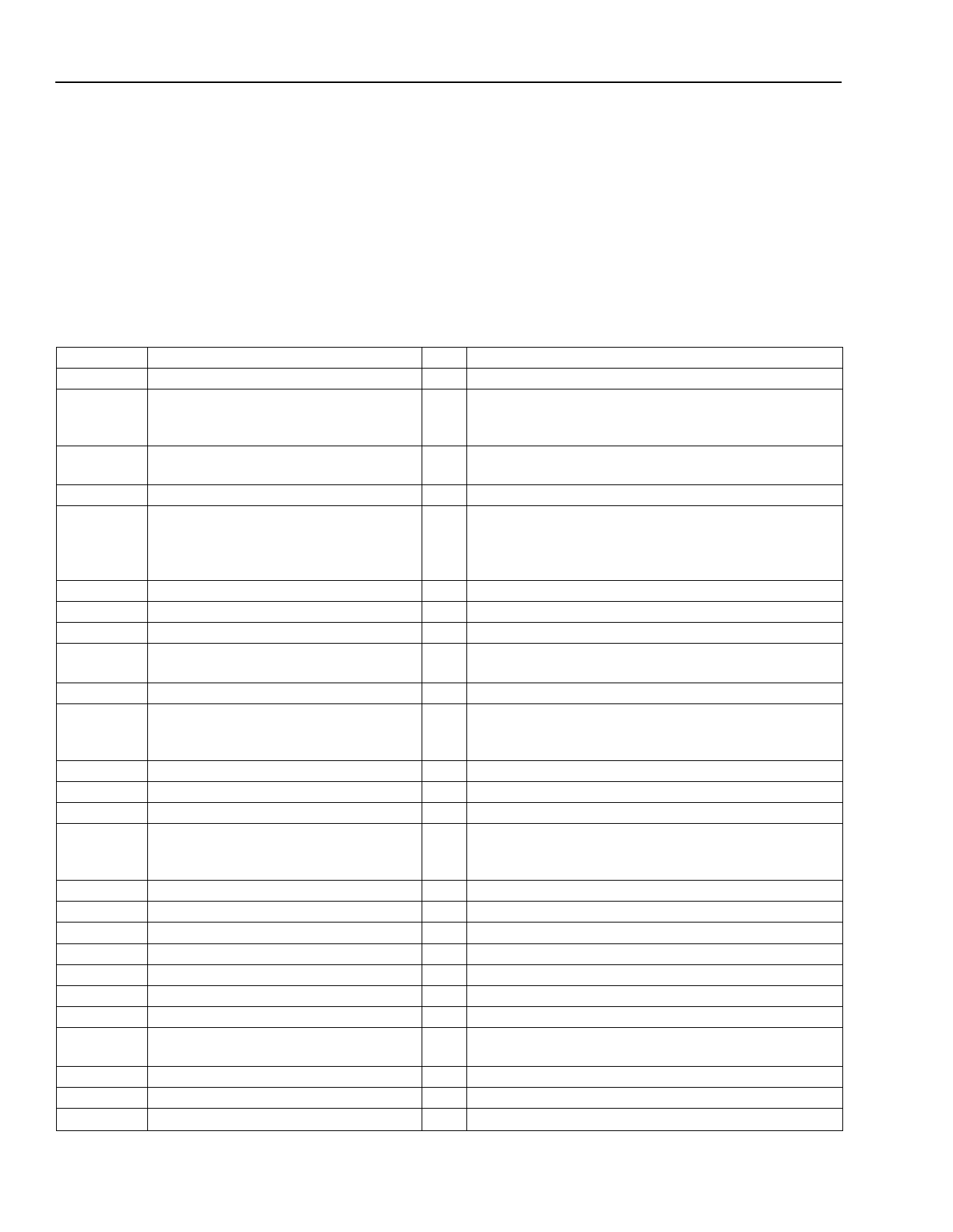
Table 2 describes the PBGA ball assignments sorted by symbol for the 208-ball package. For each signal or
power/ground connection, this table lists the PBGA coordinate, the symbol name, the type (I = input, O = output,
I/O = input/output, O/Z = 3-state output, P = power, G = ground), and description. Inputs and bidirectional pins do
not maintain full CMOS levels when not driven. They must be pulled to VDD2 or VSS through the appropriate pull
up/down resistor (refer to Section 7.1). An unused external SEMI data bus (ED[31:0]) can be statically configured
as outputs by asserting the EYMODE pin. At full CMOS levels, no significant dc current is drawn.
Table 2. 208-Ball PBGA Ball Assignments Sorted Alphabetically by Symbol
Symbol
CKI
EA[18:0]
EACKN
ECKO
ED[31:0]
EION
ERAMN
ERDY
EREQN
EROMN
ERTYPE
ERWN0
ERWN1
ESEG[3:0]
ESIZE
EXM
EYMODE
INT[3:0]
IO0BIT[6:0]
IO1BIT[6:0]
PADD[3:0]
PCSN
PD[15:0]
PIBF
PIDS
PINT
208-Ball PBGA Coordinate
H2
H15, G13, G14, G16, G15, F16, F15,
E13, E14, E16, D14, D15, D16, C16,
C15, B16, C14, A15, B14
D12
J16
B11, A11, C11, D11, B10, A10, B9, C9,
D9, D8, C8, B8, D7, C7, A7, B7, A6, B6,
D5, C5, A5, C4, A4, B4, A3, B3, A2, C3,
B1, C1, C2, D2
A14
B13
E2
E1
B12
F2
C12
A12
J14, J13, H13, H14
E3
E4
R3
J3, J2, K4, K3
N3, N1, N2, P1, P2, R1, P3
T13, T14, R14, T15, P14, R16, P15
P12, T12, P13, R13
N12
T3, R4, R5, T5, P5, N5, R6, T6, P6, N6,
R7, T7, T8, P8, N8, N9
R9
T11
P10
Type
Description
I External Clock Input.
O External Address Bus, Bits 18—0.
O External Device Acknowledge for External Memory Inter-
face (negative assertion).
O Programmable Clock Output.
I/O External Memory Data Bus, Bits 31—0.
O Enable for External I/O (negative assertion).
O External RAM Enable (negative assertion).
I External Memory Device Ready.
I External Device Request for EMI Interface (negative
assertion).
O Enable for External ROM (negative assertion).
I EROM Type Control:
If 0, asynchronous SRAM mode.
If 1, synchronous SRAM mode.
O Read/Write, Bit 0 (negative assertion).
O Read/Write, Bit 1 (negative assertion).
O External Segment Address, Bits 3—0.
I External Memory Bus Size Control:
If 0, 16-bit external interface.
If 1, 32-bit external interface.
I External Boot-up Control for CORE0.
I External Data Bus Mode Configuration Pin.
I External Interrupt Requests 3—0.
I/O BIO0 Status/Control, Bits 6—0.
I/O BIO1 Status/Control, Bits 6—0.
I PIU Address, Bits 3—0.
I PIU Chip Select (negative assertion).
I/O PIU Data Bus, Bits 15—0.
O PIU Input Buffer Full Flag.
I PIU Input Data Strobe.
O PIU Interrupt Request to Host.
8
Agere Systems Inc.
Share Link: 