MC33410FTA View Datasheet(PDF) - Motorola => Freescale
Part Name
Description
Manufacturer
MC33410FTA Datasheet PDF : 27 Pages
| |||
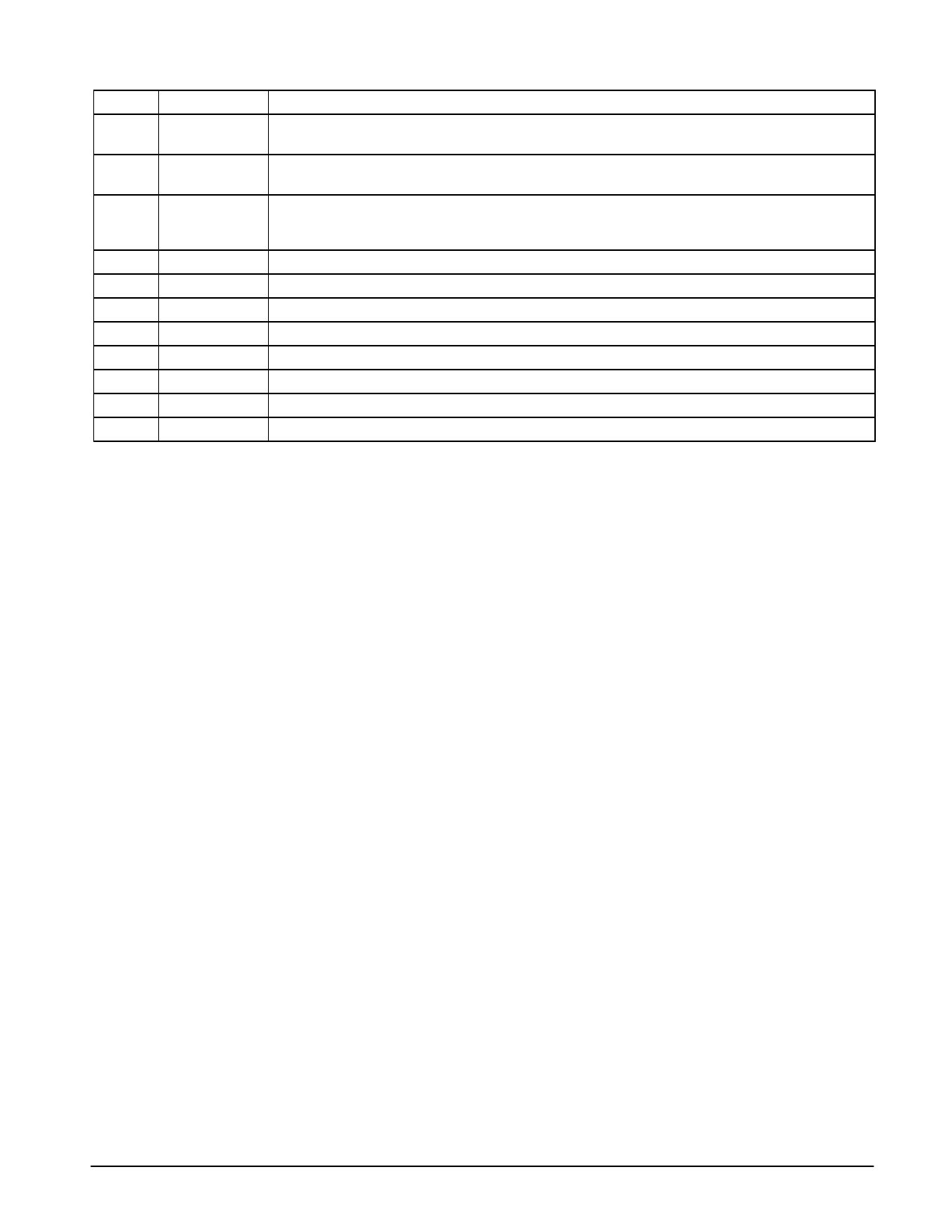
ÁÁÁÁÁÁPÁÁÁin ÁÁÁÁÁÁÁÁÁNamÁÁÁe ÁÁÁÁÁÁÁÁÁÁÁÁÁÁÁPIÁÁÁN FUÁÁÁNCÁÁÁTIOÁÁÁNMDÁÁÁCES3ÁÁCÁ3R4I1ÁÁPÁT0IOÁÁÁNDe(ÁÁÁsccornipÁÁtÁitniouneÁÁÁd) ÁÁÁÁÁÁÁÁÁÁÁÁÁÁÁÁÁÁÁÁÁÁÁÁÁÁÁÁÁÁÁÁÁ
37
VCC
Supply input for the audio sections, filters, and CVSD blocks. Allowable range is 2.7 to 5.5 V. Internally
connected to Pins 18 and 27.
38
Rx Digital Input The digital stream from the RF receiver is applied to the data slicer at this pin. Minimum amplitude is 200
mVpp. Hysteresis ≈50 mV.
39
MP2
As an output, this pin provides the recovered clock from the Clock Recovery block. As an input, the CVSD
decoder clock can be applied to this pin. Or this pin may be set to a disabled state. Selection is done
through the mP port. See Table 7. In Data Modem mode, the data to be transmitted is input to this pin.
40
Gnd
Ground for the audio sections, filters, and CVSD blocks. Internally connected to Pins 21 and 30.
41
LO2 Out
Buffered output of the 2nd LO frequency. A pullup resistor is required.
42
43, 45
LO2 VCC
LO2+, LO2–
Supply pin for the 2nd LO. Allowable range is 2.7 to 5.5 V.
A tank circuit is connected to these pins for the 2nd LO.
44
LO2 Ctl
The varactor control pin for the 2nd LO.
46
LO2 Gnd
Ground for the 2nd LO section.
47
LO2 PD
Phase detector charge pump output of the 2nd LO PLL.
48
LO2 Gnd
Ground for the 2nd LO section.
NOTE: 1. All VCC pins must be within ±0.5 V of each other.
MOTOROLA RF/IF DEVICE DATA
11
Share Link: 