ADM1021A(2012) View Datasheet(PDF) - ON Semiconductor
Part Name
Description
Manufacturer
ADM1021A Datasheet PDF : 16 Pages
| |||
ADM1021A
Table 11. DEVICE ADDRESSES (Note 1)
ADD0
ADD1
Device Address
0
0
0011 000
0
NC
0011 001
0
1
0011 010
NC
0
0101 001
NC
NC
0101 010
NC
1
0101 011
1
0
1001 100
1
NC
1001 101
1
1
1001 110
1. ADD0 and ADD1 are sampled at powerup only.
The serial bus protocol operates as follows:
1. The master initiates data transfer by establishing a
start condition, defined as a high-to-low transition
on the serial data line SDATA, while the serial
clock line SCLK remains high. This indicates that
an address/data stream will follow. All slave
peripherals connected to the serial bus respond to
the START condition and shift in the next eight
bits, consisting of a 7-bit address (MSB first) plus
an R/W bit, which determines the direction of the
data transfer, that is, whether data will be written
to or read from the slave device.
The peripheral whose address corresponds to the
transmitted address responds by pulling the data
line low during the low period before the ninth
clock pulse, known as the Acknowledge Bit. All
other devices on the bus now remain idle while the
selected device waits for data to be read from or
written to it. If the R/W bit is a 0, the master writes
to the slave device. If the R/W bit is a 1, the
master reads from the slave device.
2. Data is sent over the serial bus in sequences of
nine clock pulses, eight bits of data followed by an
Acknowledge Bit from the slave device.
Transitions on the data line must occur during the
low period of the clock signal and remain stable
during the high period, because a low-to-high
transition when the clock is high can be interpreted
as a stop signal. The number of data bytes that can
be transmitted over the serial bus in a single read
or write operation is limited only by what the
master and slave devices can handle.
3. When all data bytes have been read or written,
stop conditions are established. In write mode, the
master pulls the data line high during the 10th
clock pulse to assert a stop condition. In read
mode, the master device overrides the
acknowledge bit by pulling the data line high
during the low period before the ninth clock pulse.
This is known as No Acknowledge. The master
then takes the data line low during the low period
before the 10th clock pulse, then high during the
10th clock pulse to assert a stop condition.
Any number of bytes of data can be transferred over the
serial bus in one operation, but it is not possible to mix read
and write in one operation, because the type of operation is
determined at the beginning and cannot subsequently be
changed without starting a new operation.
For the ADM1021A, write operations contain either one
or two bytes, while read operations contain one byte.
To write data to one of the device data registers or read
data from it, the address pointer register must be set so that
the correct data register is addressed, data can then be written
into that register or read from it. The first byte of a write
operation always contains a valid address that is stored in the
address pointer register. If data is to be written to the device,
the write operation contains a second data byte that is written
to the register selected by the address pointer register.
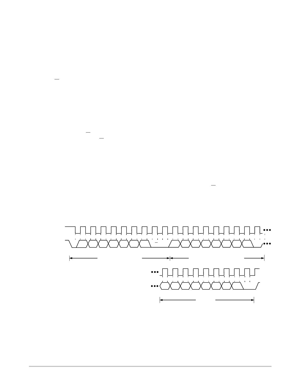
This is illustrated in Figure 14. The device address is sent
over the bus followed by R/W set to 0. This is followed by
two data bytes. The first data byte is the address of the
internal data register to be written to, which is stored in the
address pointer register. The second data byte is the data to
be written to the internal data register.
1
91
9
SCLK
SDATA
A6
START BY
MASTER
A5 A4 A3 A2 A1 A0 R/W
D7
ACK. BY
FRAME 1
ADM1021A
SERIAL BUS ADDRESS BYTE
D6 D5 D4 D3 D2 D1 D0
ACK. BY
FRAME 2
ADM1021A
ADDRESS POINTER REGISTER BYTE
1
9
SCLK (CONTINUED)
SDATA (CONTINUED)
D7 D6 D5 D4 D3 D2 D1 D0
FRAME 3
DATA BYTE
ACK. BY STOP BY
ADM1021A MASTER
Figure 14. Writing a Register Address to the Address Pointer Register, then Writing Data to the Selected Register
http://onsemi.com
11
Share Link: 