HMS97C8032 View Datasheet(PDF) - Hynix Semiconductor
Part Name
Description
Manufacturer
HMS97C8032 Datasheet PDF : 157 Pages
| |||
HMS91C8032/97C8032
HMS91C8032/HMS97C8032 Description
3. INSTRUCTION SET
The HMS9XC8032 instruction set is optimized for 8-bit control applications. It provides a variety of fast addressing modes for accessing
the internal RAM to facilitate byte operations on small data structures. The instruction set provides extensive support for one-bit variables
as a separate data type, allowing direct bit manipulation in control and logic systems that require Boolean processing.
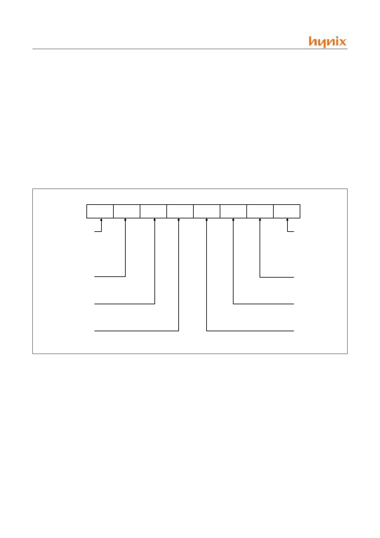
3.1 Program Status Word
The Program Status Word (PSW) contains several status bits that
reflect the current state of the CPU. The PSW, shown in Figure
3-1, resides in the SFR space. It contains the Carry bit, the Aux-
iliary Carry (for BCD operations), the two register bank select
bits, the Overflow flag, a Parity bit, and two user-definable status
flags.
The Carry bit, other than serving the functions of a Carry bit in
arithmetic operations, also serves as the “Accumulator” for a
number of Boolean operations.
CY
AC
F0
RS1
RS0
OV
-
PSW 7
Carry flag receives carry out
from bit 7 of ALU operands
PSW 6
Auxiliary carry flag receives
carry out from bit 3
of addition operands
PSW 5
General purpose status flag
PSW 4
Register bank select bit 1
P
PSW 0
Parity of accumulator
set by hardware to 1 if it
contains an odd number
of 1s; otherwise it is
reset to 0
PSW 1
User-definable flag
PSW 2
Overflow flag set by
arithmetic operation
PSW 3
Register bank select bit 0
Figure 3-1 PSW (Program Status Word) Register in HMS9XC8032 Devices
RS0 and RS1 are used to select one of the four register banks.
Each register bank composed of eight registers.(R0 to R7) The
selection of a register bank is made at execution time.
The parity bit reflects the number of 1s in the Accumulator: P= 1
if the Accumulator contains an odd number of 1s, and P = 0 if the
Accumulator contains an even number of 1s. Thus the number of
1s in the Accumulator plus P is always even. Two bits in the PSW
are uncommitted and may be used as general-purpose status
flags.
Direct Addressing
In direct addressing the operand is specified by an 8-bit address
field in the instruction. Only internal Data RAM and SFRs can be
directly addressed.
Indirect Addressing
In indirect addressing the instruction specifies a register which
contains the address of the operand. Both internal and external
RAM can be indirectly addressed.
3.2 Addressing Modes
The addressing modes in the HMS9XC8032 instruction set are as
follows:
The address register for 8-bit addresses can be R0 or R1 of the se-
lected bank, or the Stack Pointer. The address register for 16-bit
addresses can only be the 16-bit "data pointer" register, DPTR.
8
NOV., 2001 Ver 1.02
Share Link: 