M34282M1 View Datasheet(PDF) - Renesas Electronics
Part Name
Description
Manufacturer
M34282M1 Datasheet PDF : 69 Pages
| |||
4282 Group
CLOCK CONTROL
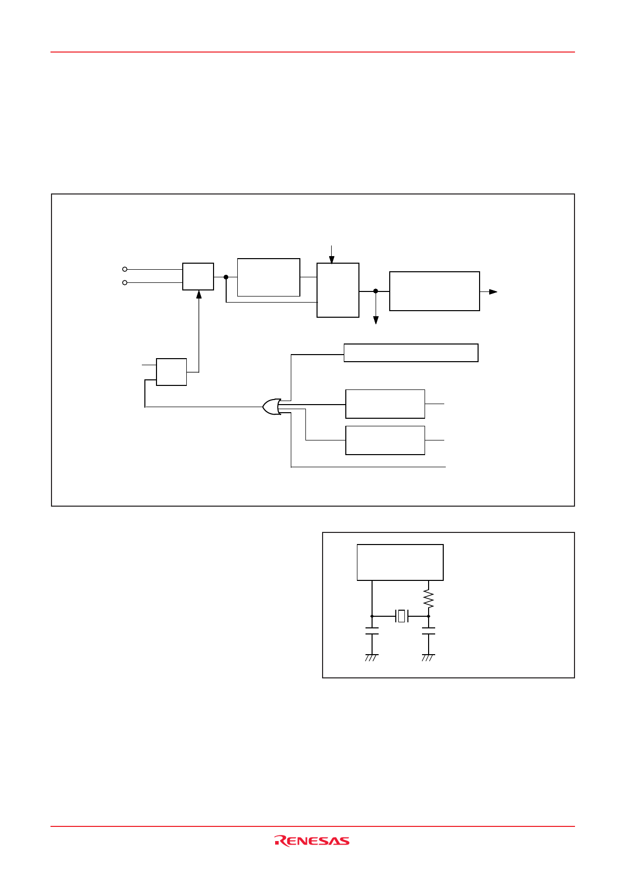
The clock control circuit consists of the following circuits.
• System clock generating circuit
• Control circuit to stop the clock oscillation
• Control circuit to return from the RAM back-up state
XI N
XOUT
OSC
POF instruction
R
Q
S
CCK instruction
Frequency
divider
(divided by 8)
Multi-
plexer
Internal clock
generation circuit
(divided by 4)
STCK
Internal power-on reset circuit
INSTCK
Pull-down control
register PU0
Pull-down control
register 1
Ports E0,E1,G0–G3
Ports D4–D7
Port E2
Fig. 26 Clock control circuit structure
System clock signal f(XIN) is obtained by externally connecting a
ceramic resonator. Connect this external circuit to pins XIN and
XOUT at the shortest distance as shown Figure 27.
A feedback resistor is built-in between XIN pin and XOUT pin.
ROM ORDERING METHOD
Please submit the information described below when ordering
Mask ROM.
(1) Mask ROM Order Confirmation Form*
(2) Mark Specification Form
(3) Data to be written to ROM, in EPROM form (three identical
copies) or one floppy disk.
XIN
4
CIN
4282
XOUT
5
Use the resonator
manufacturer’s
recommended value
because constants
such as capacitance
depend on the
resonator.
COUT
* For the mask ROM confirmation and the mark specifications,
refer to the “Renesas Technology Corp.” Homepage
(http://www.renesas.com/en/rom).
Fig. 27 Ceramic resonator external circuit
Rev.1.33 Mar 18, 2004 page 21 of 67
Share Link: 