MT6162 View Datasheet(PDF) - MediaTek Inc
Part Name
Description
Manufacturer
MT6162 Datasheet PDF : 32 Pages
| |||
MT6162
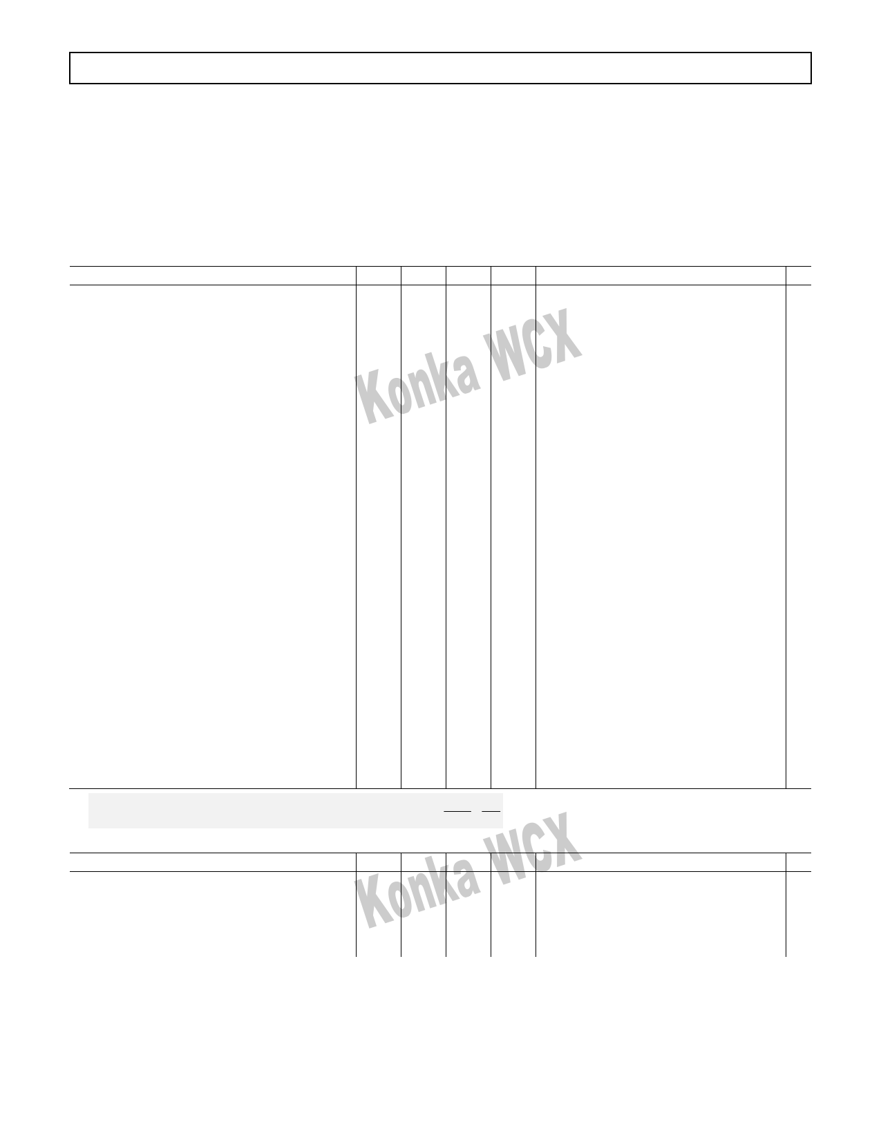
ELECTRICAL CHARACTERISTICS
The Electrical Characteristics defined are valid for the Operating Conditions specified in Table 1, receiver pin configuration#1, and
transmitter pin configuration#1, unless otherwise described. For ABB gain blocks settings based on a specific ABB gain. The dc-dc
converter supplying VDD_18 is assumed to have 90% efficiency and operates from a nominal battery voltage, Vbat ~ 3.6V.
Typical specifications are for register settings are mid-band channel frequencies, and recommended operating conditions. Min/Max
specifications are for Extreme operating voltage and temperature conditions, unless otherwise stated.
DC & VOLTAGE REGULATORS
Table 8
Parameter
Min Typ Max Unit Test Conditions / Comments
Idle mode
Equivalent Battery Supply Current 3)
Rx Alert
Rx On
3G mode, max gain
3G mode, med gain
3G mode, low gain
GGE mode, max gain
GGE mode, med gain
GGE mode, low gain
Tx Alert
Tx (HB) On
WCDMA mode @ Pout = +4.5dBm
WCDMA mode @ Pout = +2.5dBm
WCDMA mode @ Pout = -10dBm
WCDMA mode @ Pout ≤ -58dBm
GMSK mode
8PSK mode @ Pout = -2.5dBm
MMMB GMSK mode
MMMB 8PSK mode @ Pout = +3.5dBm
Tx (LB) On
WCDMA mode @ Pout = +2.5dBm
WCDMA mode @ Pout = -10dBm
WCDMA mode @ Pout ≤ -58dBm
GMSK mode
8PSK mode @ Pout = +0.5dBm
MMMB GMSK mode
MMMB 8PSK mode @ Pout = +4.5dBm
11
μA VINT on; All else off
Konka_WCXVDD_18 & VDD_28
3.3 4 mA All Rx power domain LDOs enabled
RX signal path fully enabled; Tx off
38 48 mA LNA HI gain/ ABB gain: 32dB
31 40 mA LNA MED gain/ ABB gain: 14dB
28 35 mA LNA LOW gain/ ABB gain: -7dB
40 50 mA LNA HI gain/ ABB gain: 32dB
33 41 mA LNA MED gain/ ABB gain: 14dB
30 37.5 mA LNA LOW gain/ ABB gain: -7dB
2
3 mA All Tx power domain LDOs enabled
Tx high-band signal path on; Rx off
92 112 mA 12.2k UL ref ch. (187mVd rms I/Q)
91 110 mA 12.2k UL ref ch. (187mVd rms I/Q)
51 62 mA 12.2k UL ref ch. (187mVd rms I/Q)
34 43 mA 12.2k UL ref ch. (187mVd rms I/Q)
35 44 mA TX_HB1 output
64 80 mA TX_HB1 output; (180mVd rms I/Q)
94
mA TYP output power; RF gain = 1
83 104 mA
Tx low-band signal path on; Rx off
75 94 mA 12.2k UL ref ch. (187mVd rms I/Q)
40 50 mA 12.2k UL ref ch. (187mVd rms I/Q)
34 43 mA 12.2k UL ref ch. (187mVd rms I/Q)
36 45 mA TX_LB2 output
71 89 mA TX_LB2 output; (180mVd rms I/Q)
87
mA TYP output power; RF gain = 1
90 110 mA
3) equivalent _ battery _ current = Idd(VDD _ 28) + Idd(VDD _18)× 1.8V × 1
Table 9
Parameter
VDDXO Supply Current
External clock mode
Konka_WCX 3.6V 0.9
Min Typ Max Unit Test Conditions / Comments
2.2
mA REFCLK1 output enabled with DS load
condition; AFC DAC turned off
DCXO mode
3.5
mA REFCLK1 output enabled with DS load
condition; AFC DAC turned off
REV. (1.5) Mar 20th 2011
- 11 - MediaTek Proprietary & Confidential Information
Share Link: 