ADF7020BCP View Datasheet(PDF) - Analog Devices
Part Name
Description
Manufacturer
ADF7020BCP Datasheet PDF : 40 Pages
| |||
Preliminary Technical Data
FREQUENCY SYNTHESIZER
REFERENCE INPUT SECTION
The on-board crystal oscillator circuitry (Figure 5) can use an
inexpensive quartz crystal as the PLL reference. The oscillator
circuit is enabled by setting R1_DB12 high. It is enabled by
default on power-up and is disabled by bringing CE low. Errors
in the crystal can be corrected using the automatic frequency
control (see the AFC Section) feature or by adjusting the
fractional-N value (see the N Counter section). A single-ended
reference (TCXO, CXO) can also be used. The CMOS levels
should be applied to OSC2 with R1_DB12 set low.
OSC1
OSC2
CP2
CP1
Figure 5. Oscillator Circuit on the ADF7020
Two parallel resonant capacitors are required for oscillation at
the correct frequency; their values are dependent on the crystal
specification. They should be chosen so that the series value of
capacitance added to the PCB track capacitance adds up to the
load capacitance of the crystal, usually 20 pF. Track capacitance
values vary from 2 pF to 5 pF, depending on board layout.
Where possible, choose capacitors that have a very low
temperature coefficient to ensure stable frequency operation
over all conditions.
CLKOUT Divider and Buffer
The CLKOUT circuit takes the reference clock signal from the
oscillator section, shown in Figure 5, and supplies a divided-
down 50:50 mark-space signal to the CLKOUT pin. An even
divide from 2 to 30 is available. This divide number is set in
R1_DB(8:11). On power-up, the CLKOUT defaults to
divide-by-8.
DVDD
CLKOUT
ENABLE BIT
OSC1
DIVIDER
1 TO 15
÷2
CLKOUT
Figure 6. CLKOUT Stage
To disable CLKOUT, set the divide number to 0. The output
buffer can drive up to a 20 pF load with a 10% rise time at
4.8 MHz. Faster edges can result in some spurious feedthrough
to the output. A small series resistor (50 Ω) can be used to slow
the clock edges to reduce these spurs at FCLK.
ADF7020
R Counter
The 3-bit R counter divides the reference input frequency by an
integer from 1 to 7. The divided-down signal is presented as the
reference clock to the phase frequency detector (PFD). The
divide ratio is set in Register 1. Maximizing the PFD frequency
reduces the N value. This reduces the noise multiplied at a rate
of 20 log(N) to the output, as well as reducing occurrences of
spurious components. The R Register defaults to R = 1 on
power-up:
PFD [Hz] = XTAL/R
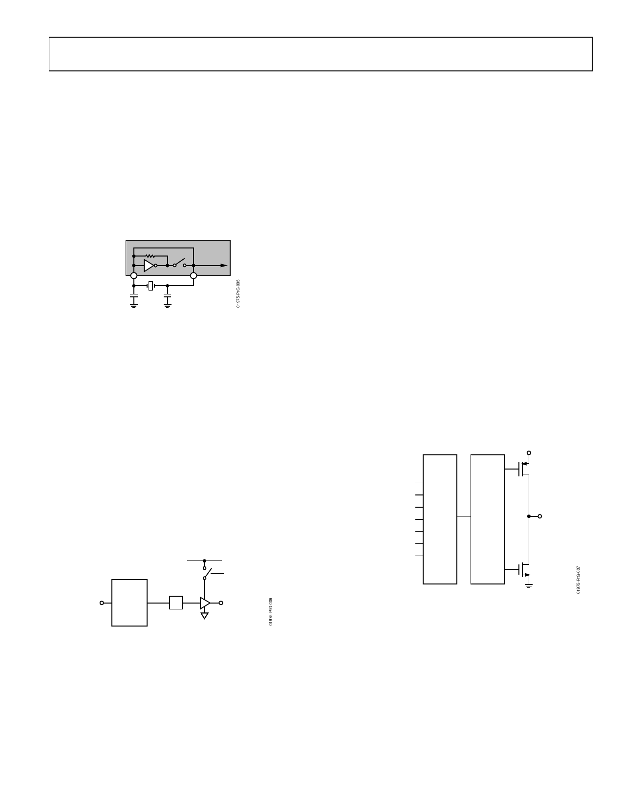
MUXOUT and Lock Detect
The MUXOUT pin allows the user to access various digital
points in the ADF7020. The state of MUXOUT is controlled by
Bits R0_DB(29:31).
Regulator Ready
REGULATOR READY is the default setting on MUXOUT after
the transceiver has been powered up. The power-up time of the
regulator is typically 50 µs. Because the serial interface is
powered from the regulator, the regulator must be at its nominal
voltage before the ADF7020 can be programmed. The status of
the regulator can be monitored at MUXOUT. When the
REGULATOR READY signal on MUXOUT is high,
programming of the ADF7020 can begin.
DVDD
REGULATOR READY
DIGITAL LOCK DETECT
ANALOG LOCK DETECT
R COUNTER OUTPUT
N COUNTER OUTPUT
PLL TEST MODES
Σ-∆ TEST MODES
MUX
CONTROL
MUXOUT
DGND
Figure 7. MUXOUT Circuit
Digital Lock Detect
Digital lock detect is active high. The lock detect circuit is
located at the PFD. When the phase error on five consecutive
cycles is less than 15 ns, lock detect is set high. Lock detect
remains high until 25 ns phase error is detected at the PFD.
Because no external components are needed for digital lock
detect, it is more widely used than analog lock detect.
Rev. PrH | Page 11 of 40
Share Link: 