SST25VF032B View Datasheet(PDF) - Silicon Storage Technology
Part Name
Description
Manufacturer
SST25VF032B Datasheet PDF : 28 Pages
| |||
32 Mbit SPI Serial Flash
SST25VF032B
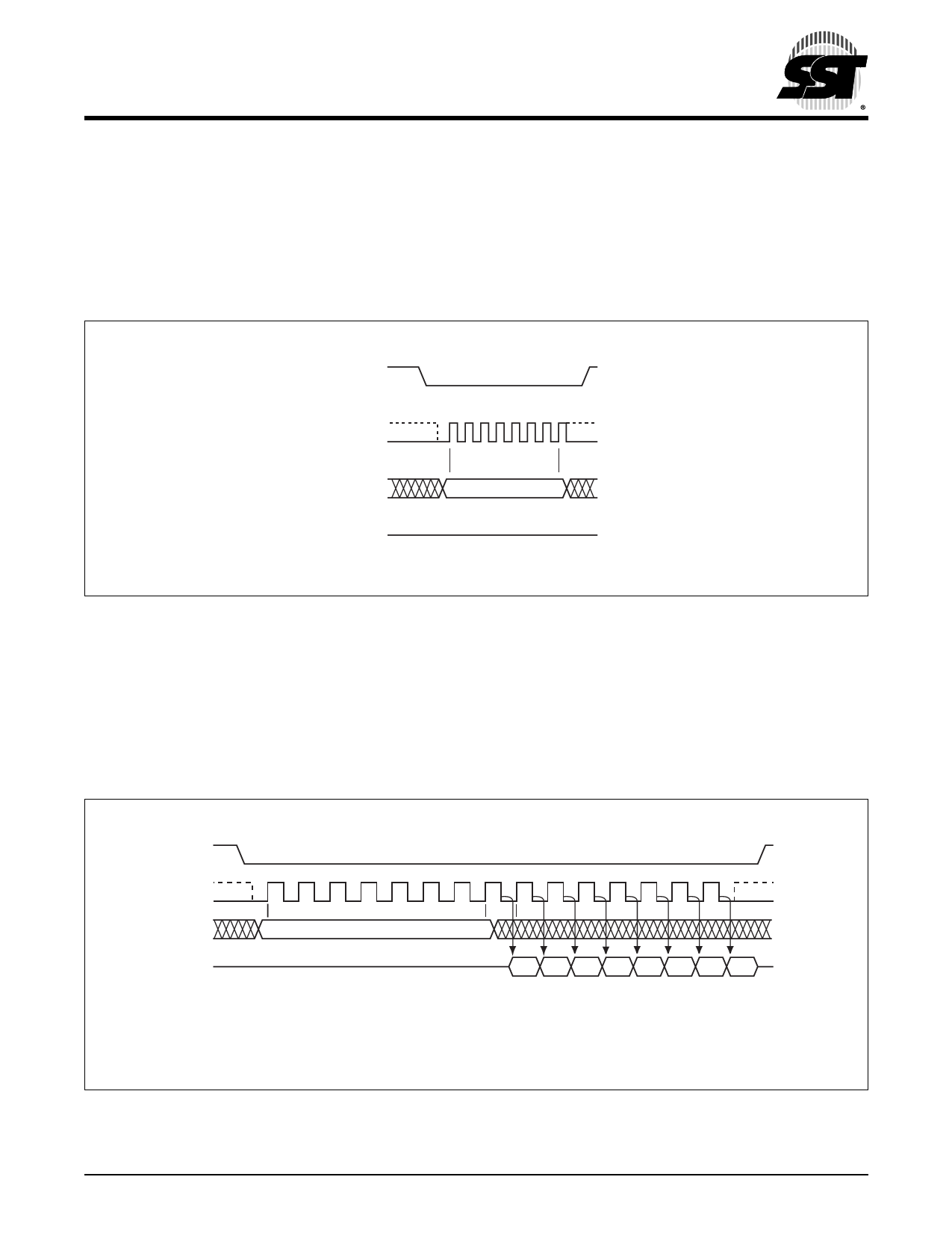
Chip-Erase
The Chip-Erase instruction clears all bits in the device to
FFH. A Chip-Erase instruction will be ignored if any of the
memory area is protected. Prior to any Write operation, the
Write-Enable (WREN) instruction must be executed. CE#
must remain active low for the duration of the Chip-Erase
instruction sequence. Initiate the Chip-Erase instruction by
Data Sheet
executing an 8-bit command, 60H or C7H. CE# must be
driven high before the instruction is executed. Poll the Busy
bit in the software status register or wait TCE for the comple-
tion of the internal self-timed Chip-Erase cycle. See Figure
15 for the Chip-Erase sequence.
CE#
MODE 3
SCK MODE 0
0 1 2345 6 7
SI
60 or C7
MSB
SO
HIGH IMPEDANCE
1327 F16.0
FIGURE 15: Chip-Erase Sequence
Read-Status-Register (RDSR)
The Read-Status-Register (RDSR) instruction allows read-
ing of the status register. The status register may be read at
any time even during a Write (Program/Erase) operation.
When a Write operation is in progress, the Busy bit may be
checked before sending any new commands to assure that
the new commands are properly received by the device.
CE# must be driven low before the RDSR instruction is
entered and remain low until the status data is read. Read-
Status-Register is continuous with ongoing clock cycles
until it is terminated by a low to high transition of the CE#.
See Figure 16 for the RDSR instruction sequence.
CE#
MODE 3 0
1
2
3
4
5
6
7
8
9 10 11 12 13 14
SCK MODE 0
SI
05
MSB
HIGH IMPEDANCE
SO
Bit 7 Bit 6 Bit 5 Bit 4 Bit 3 Bit 2 Bit 1 Bit 0
MSB
Status
Register Out
1327 F17.0
FIGURE 16: Read-Status-Register (RDSR) Sequence
©2009 Silicon Storage Technology, Inc.
15
S71327-03-000
05/09
Share Link: 