APA300-BG View Datasheet(PDF) - Unspecified
Part Name
Description
Manufacturer
APA300-BG Datasheet PDF : 174 Pages
| |||
ProASICPLUS Flash Family FPGAs
enable the user to define a wide range of frequency
multipliers and divisors. The clock conditioning circuit can
advance or delay the clock up to 8 ns (in increments of
0.25 ns) relative to the positive edge of the incoming
reference clock. The system also allows for the selection of
output frequency clock phases of 0┬░ and 180┬░.
Prior to the application of signals to the rib drivers, they
pass through programmable delay units, one per global
network. These units permit the delaying of global
signals relative to other signals to assist in the control of
input set-up times. Not all possible combinations of input
and output modes can be used. The degrees of freedom
available in the bidirectional global pad system and in
the clock conditioning circuit have been restricted. This
avoids unnecessary and unwieldy design kit and software
work.
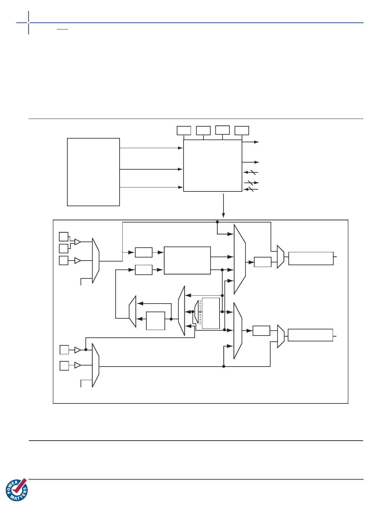
AVDD AGND VDD GND
Global MUX B OUT
GLA
Input Pins to the PLL
See Figure 1-15
on pa+ge 1-14
-
External Feedback Signal
Global MUX A OUT
Clock Conditioning
Circuitry
(Top level view)
GLB
27 Flash
4 Configuration Bits
Dynamic
Configuration Bits
8
Clock Conditioning Circuitry Detailed Block Diagram
CLK
Bypass Primary
P+
P-
Clock from Core
(GLINT mode)
EXTFB
FIVDIV[4:0]
├Ęn
├Ęm
FBDIV[5:0]
PLL Core
180˚
0˚
0
1
XDLYSEL
Deskew
Delay
2.95 ns
1
Delay Line
0.25 ns to
2
4.00 ns,
16 steps,
0.25 ns
3
increments
FBDLY[3:0]
FBSEL[1:0]
OBMUX[2:0]
1
7
0
DLYB[1:0]
6
Delay Line 0.0 ns, 0.25 ns, GLB
5
├Ęu
0.50 ns and 4.00 ns
4 OBDIV[1:0]
2
3
OADIV[1:0]
2
├Ęv
1
OAMUX[1:0]
DLYA[1:0]
Delay Line 0.0 ns, 0.25 ns,
0.50 ns and 4.00 ns
GLA
CLKA
Clock from Core
(GLINT mode)
Bypass Secondary
Notes:
1. FBDLY is a programmable delay line from 0 to 4 ns in 250 ps increments.
2. DLYA and DLYB are programmable delay lines, each with selectable values 0 ps, 250 ps, 500 ps, and 4 ns.
3. OBDIV will also divide the phase-shift since it takes place after the PLL Core.
Figure 1-14 ŌĆó PLL Block ŌĆō Top-Level View and Detailed PLL Block Diagram
1-14
v5.7
Share Link: 