MC13191 View Datasheet(PDF) - Freescale Semiconductor
Part Name
Description
Manufacturer
MC13191 Datasheet PDF : 24 Pages
| |||
MCU
MC13191
Shift Register
RxD
TxD
MISO
MOSI
Shift Register
Sclk
SPICLK
Baud Rate
Generator
Chip Enable (CE)
CE
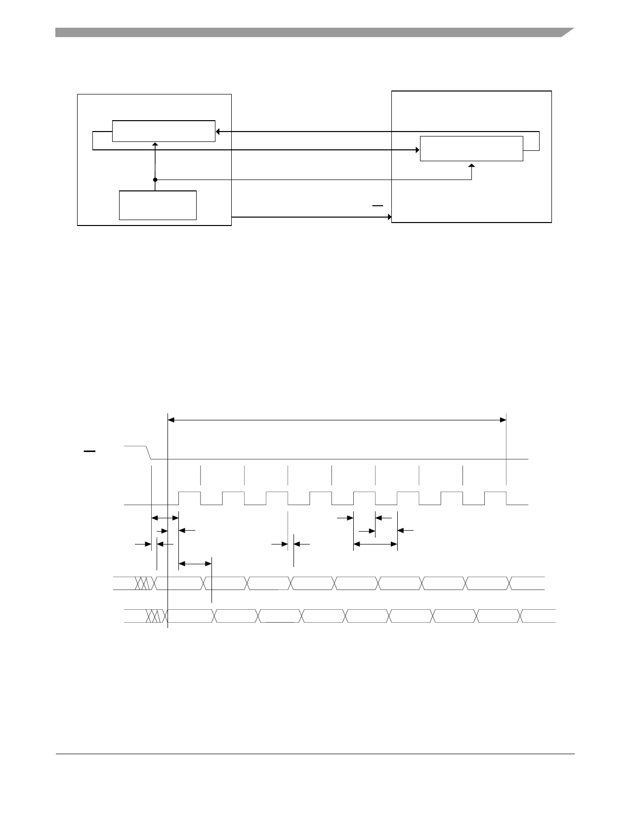
Figure 6. SPI Interface
Although the SPI port is fully static, internal memory, timer, and interrupt arbiters require an internal clock
(CLKcore) derived from the crystal reference oscillator, to communicate from the SPI registers to internal
registers and memory.
6.2.1 SPI Burst Operation
The SPI port of an MCU transfers data in bursts of 8 bits with most significant bit (MSB) first. The master
(MCU) can send a byte to the slave (transceiver) on the MOSI line and the slave can send a byte to the
master on the MISO line. Although an MC13191 transaction is three or more SPI bursts long, the timing
of a single SPI burst is shown in Figure 6.
SPI Burst
CE
SPICLK
T5
MISO
1
2
3
4
5
6
7
8
T4
T6
T7
Valid
Valid
T2
T1
T3
T0
MOSI
Valid
Figure 7. SPI Single Burst Timing Diagram.
SPI digital timing specifications are shown in Table 6.
MC13191 Technical Data, Rev. 1.6
Freescale Semiconductor
11
Share Link: 