LC75817NW View Datasheet(PDF) - SANYO -> Panasonic
Part Name
Description
Manufacturer
LC75817NW
SANYO -> Panasonic

LC75817NW Datasheet PDF : 43 Pages
| |||
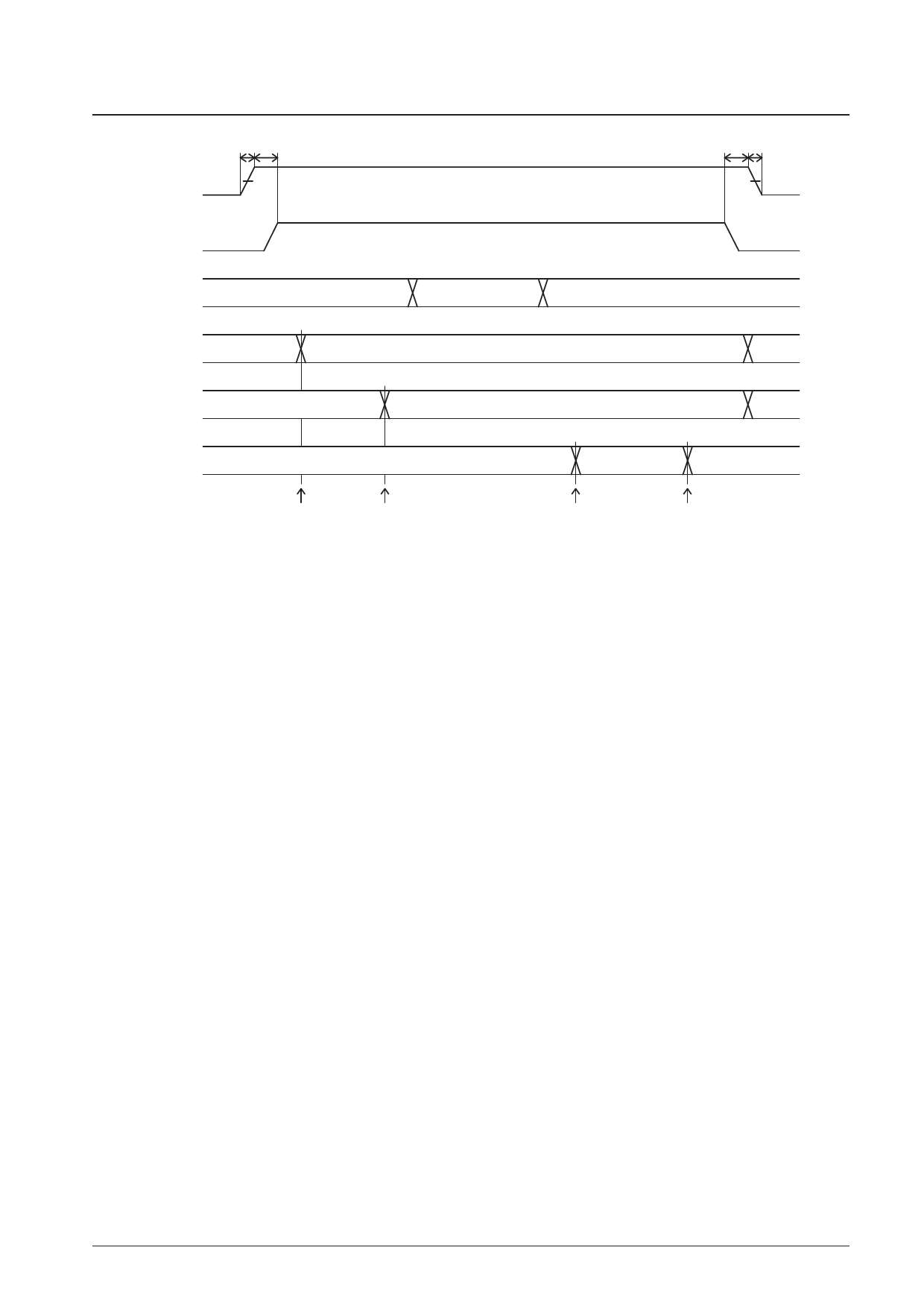
VDD
VLCD
t1 t2
VDET
Instruction execution
LC75817NE, 75817NW
Initial state settings
t3 t4
VDET
Key scan
Disabled
General-purpose
output ports
Fixed at the low level (VSS)
Display state
Execution enabled
Can be set to either the high (VDD), or low (VSS) level
Display off
Display on
Display off
“Set key scan output “Set general-purpose
state” instruction output port state”
execution
instruction execution
“Display on/off control”
instruction execution
(Turning the display on)
”Display on/off control“
instruction execution
(Turning the display off)
• t1 ≥ 1 ms (Logic block power supply voltage VDD rise time)
• t2 ≥ 0 ms
• t3 ≥ 0 ms
• t4 ≥ 1 ms (Logic block power supply voltage VDD fall time)
• Initial state settings
Set display technique
DCRAM data write
ADRAM data write (If the ADRAM is used.)
CGRAM data write (If the CGRAM is used.)
Set AC address
Set display contrast (If the display contrast adjustment circuit is used.)
Figure 3
No. 6144-28/43
Share Link: