LC75817NW View Datasheet(PDF) - SANYO -> Panasonic
Part Name
Description
Manufacturer
LC75817NW
SANYO -> Panasonic

LC75817NW Datasheet PDF : 43 Pages
| |||
LC75817NE, 75817NW
Electrical Characteristics for the Allowable Operating Ranges
Parameter
Hysteresis
Power-down detection voltage
Input high level current
Input low level current
Input floating voltage
Pull-down resistance
Output off leakage current
Output high level voltage
Output low level voltage
Output middle level voltage*2
Oscillator frequency
Current drain
Symbol
Conditions
VH
VDET
IIH
IIL
VIF
RPD
IOFFH
VOH1
VOH2
VOH3
VOH4
VOH5
VOL1
VOL2
VOL3
VOL4
VOL5
VOL6
VMID1
VMID2
VMID3
fOSC
IDD1
IDD2
ILCD1
ILCD2
CE, CL, DI, INH, KI1 to KI5
CE, CL, DI, INH, OSCI: VI = 6.0 V
CE, CL, DI, INH, OSCI: VI = 0 V
KI1 to KI5
KI1 to KI5: VDD = 5.0 V
DO: VO = 6.0 V
S1 to S60: IO = –20 µA
COM1 to COM10: IO = –100 µA
KS1 to KS6: IO = –500 µA
P1 to P4: IO = –1 mA
OSCO: IO = –500 µA
S1 to S60: IO = 20 µA
COM1 to COM10: IO = 100 µA
KS1 to KS6: IO = 25 µA
P1 to P4: IO = 1 mA
OSCO: IO = 500 µA
DO: IO = 1 mA
S1 to S60: IO = ±20 µA
COM1 to COM10: IO = ±100 µA
COM1 to COM10: IO = ±100 µA
OSCI, OSCO: ROSC = 33 kΩ, COSC = 220 pF
VDD: sleep mode
VDD: VDD = 6.0 V, output open, fOSC = 300 kHz
VLCD: sleep mode
VLCD: VLCD = 10.0 V, output open, fOSC = 300 kHz
When the display contrast adjustment circuit is used.
Ratings
Unit
min
typ
max
0.1 VDD
2.5
3.0
V
3.5 V
5.0 µA
–5.0
µA
0.05 VDD V
50
100
250 kΩ
6.0 µA
VLCD0 – 0.6
VLCD0 – 0.6
VDD – 1.0 VDD – 0.5
VDD – 0.2 V
VDD – 1.0
VDD – 1.0
VLCD4 + 0.6
VLCD4 + 0.6
0.2
0.5
1.5
V
1.0
1.0
0.1
0.5
2/4 (VLCD0 – VLCD4) – 0.6
3/4 (VLCD0 – VLCD4) – 0.6
1/4 (VLCD0 – VLCD4) – 0.6
210
300
2/4 (VLCD0 – VLCD4) + 0.6
3/4 (VLCD0 – VLCD4) + 0.6
1/4 (VLCD0 – VLCD4) + 0.6
390
V
kHz
100
500
1000
5
450
900 µA
ILCD3
VLCD: VLCD = 10.0 V, output open, fOSC = 300 kHz
When the display contrast adjustment circuit is not used.
200
400
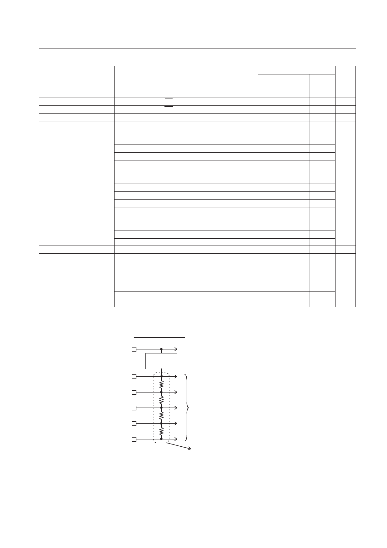
Note: *2. Excluding the bias voltage generation divider resistor built into the VLCD0, VLCD1, VLCD2, VLCD3, and VLCD4. (See Figure 1.)
VLCD
VLCD0
VLCD1
VLCD2
VLCD3
VLCD4
CONTRAST
ADJUSTER
To the common and segment drivers
Excluding these resistors
Figure 1
No. 6144-5/43
Share Link: