7C1325-100(2000) View Datasheet(PDF) - Cypress Semiconductor
Part Name
Description
Manufacturer
7C1325-100 Datasheet PDF : 16 Pages
| |||
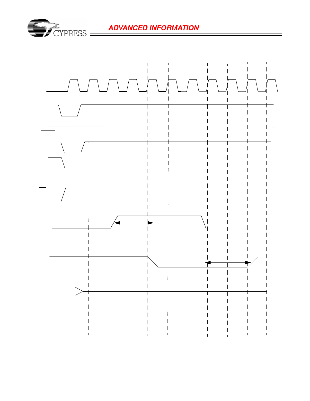
Timing Diagrams (continued)
Read/Write Cycle Timing
CY7C1325
CLK
tCH
tCYC
tCL
ADD
tAS
A
ADSP
tADS
ADSC
tAH
B
tADS
C
D
tADH
tADH
ADV
tADVS
tADVH
CE1
CE
tCES
tCES
tCEH
tCEH
tWES
tWEH
WE
ADSP ignored
OE
with CE1 HIGH
tCLZ
Data
In/Out
tCDV
Q(A)
Q(B)
Q
Q
(B+1) (B+2)
Q
(B+3)
Q(B)
tEOHZ
D(C)
D
D
D
(C+1) (C+2) (C+3)
tDOH
tCHZ
Q(D)
Device originally
deselected
WE is the combination of BWE, BWS[1:0], and GW to define a write cycle (see Write Cycle Descriptions table).
CE is the combination of CE2 and CE3. All chip selects need to be active in order to select
the device. RAx stands for Read Address X, WAx stands for Write Address X, Dx stands for Data-in X,
Qx stands for Data-out X.
12
Share Link: 