ILX511 View Datasheet(PDF) - Sony Semiconductor
Part Name
Description
Manufacturer
ILX511 Datasheet PDF : 13 Pages
| |||
ILX511
Electro-optical Characteristics
(Ta = 25 °C, VDD = 5 V, Clock frequency: 1 MHz, Light source = 3200 K, IR cut filter: CM-500S (t = 1.0 mm),
Without S/H mode)
Item
Symbol
Min.
Typ.
Max.
Unit
Remarks
Sensitivity 1
R1
150
200
250
V/(lx • s) Note 1
Sensitivity 2
R2
—
1800
—
V/(lx • s) Note 2
Sensitivity nonuniformity
PRNU
—
5.0
10.0
%
Note 3
Saturation output voltage
VSAT
0.6
0.8
—
V
—
Dark voltage average
VDRK
—
3.0
6.0
mV
Note 4
Dark signal nonuniformity
DSNU
—
6.0
12.0
mV
Note 4
Image lag
IL
—
1
—
%
Note 5
Dynamic range
DR
—
267
—
—
Note 6
Saturation exposure
SE
—
0.004
—
lx • s
Note 7
5 V current consumption
I VDD
—
5.0
10.0
mA
—
Total transfer efficiency
TTE
92.0
98.0
—
%
—
Output impedance
ZO
—
250
—
Ω
—
Offset level
VOS
—
2.8
—
V
Note 8
Note)
1. For the sensitivity test light is applied with a uniform intensity of illumination.
2. Light source: LED λ = 660nm
3. PRNU is defined as indicated below. Ray incidence conditions are the same as for Note 1.
(VMAX-VMIN)/2
PRNU =
× 100 (%)
VAVE
The maximum output of all the valid pixels is set to VMAX, the minimum output to VMIN and the average
output to VAVE.
4. Integration time is 10ms.
5. Typical value is used for clock pulse and readout pulse. VOUT = 500 mV.
6. DR = VSAT/VDRK. When optical integration time is shorter, the dynamic range sets wider because dark
voltage is in proportion to optical integration time.
7. SE = VSAT/R1
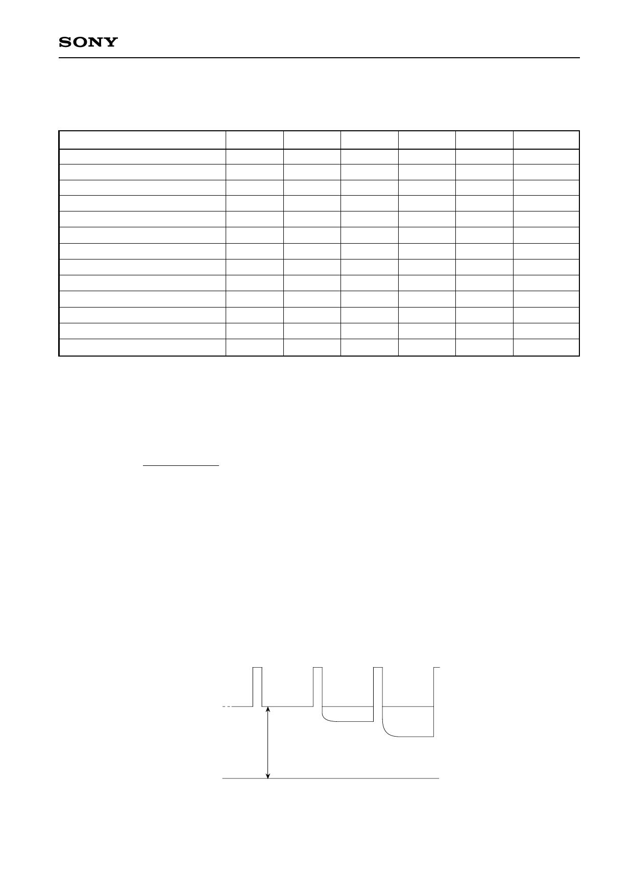
8. Vos is defined as indicated below.
D30
D31
D32
S1
VOUT
Vos
GND
—3—
Share Link: 