MSM9810B View Datasheet(PDF) - Oki Electric Industry
Part Name
Description
Manufacturer
MSM9810B Datasheet PDF : 45 Pages
| |||
OKI Semiconductor
FEDL9810BFULL-03
MSM9810B
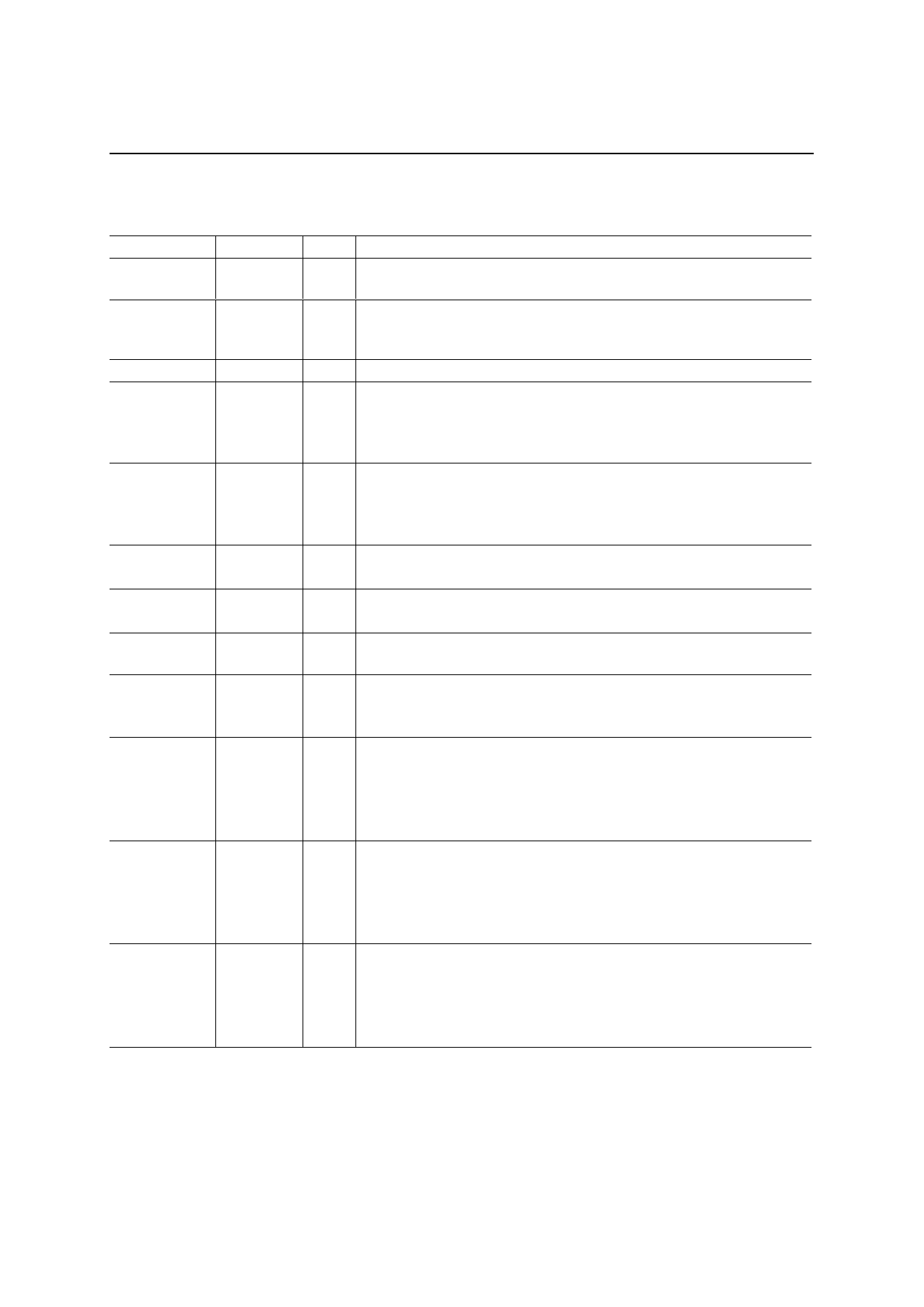
PIN DESCRIPTIONS
Pin
40-47, 49-64
30, 31, 33-38
39
8
15
16
18
20
14
28
27
26
Symbol
RA23-RA0
RD7-RD0
ROE
RCS
CMD
RD
WR
CS
SERIAL
D7/SD
D6/SI
D5/SO
Type
O
I
O
I
I
I
I
I
I
I/O
I/O
I/O
Description
Address pins for external memory. These pins become high impedance
when RCS pin is “H“.
Data pin for external memory. Pull-down resistors are internally
connected to these pins. These pull-down resistors become valid when
the RCS pin is “H”, and become invalid when the RCS pin is “L”.
Output enable pin for external memory.
When this pin is “L”, RA23 to RA0 and ROE pins output address data
and output enable signal.
When this pin is “H”, RA23 to RA0 and ROE pins become high
impedance.
Select pin for Command data or Subcommand data for CPU interface.
When this pin is “H”, subcommand input is selected.
When this pin is “L”, command input is selected. A pull-up resistor is
internally connected to this pin.
Read pin for CPU interface.
A pull-up resistor is internally connected to this pin.
Write pin for CPU interface.
A pull-up resistor is internally connected to this pin.
Chip select pin for CPU interface. When CS is “H”, WR/RD signal is not
entered in this LSI. A pull-up resistor is internally connected to this pin.
CPU input interface select pin. When SERIAL is “H”, serial input
interface is selected.
When it is “L”, parallel input interface is selected.
Data bus pin for CPU interface when parallel input interface is selected.
When WR is “L”, this pin serves as data input pin.
When RD is “L”, this pin serves as channel status data output pin.
When serial input interface is selected, this pin serves as serial data
input pin.
Data bus pin for CPU interface when parallel input interface is selected.
When WR is “L”, this pin serves as data input pin.
When RD is “L”, this pin serves as channel status output pin.
When serial input interface is selected, this pin serves as serial clock
input pin.
Data bus pin for CPU interface when parallel input interface is selected.
When WR is “L”, this pin serves as data input pin.
When RD is “L”, this pin serves as channel status output pin.
When serial input interface is selected, this pin serves as channel status
serial output pin.
4/45
Share Link: 