MSM9810B View Datasheet(PDF) - Oki Electric Industry
Part Name
Description
Manufacturer
MSM9810B Datasheet PDF : 45 Pages
| |||
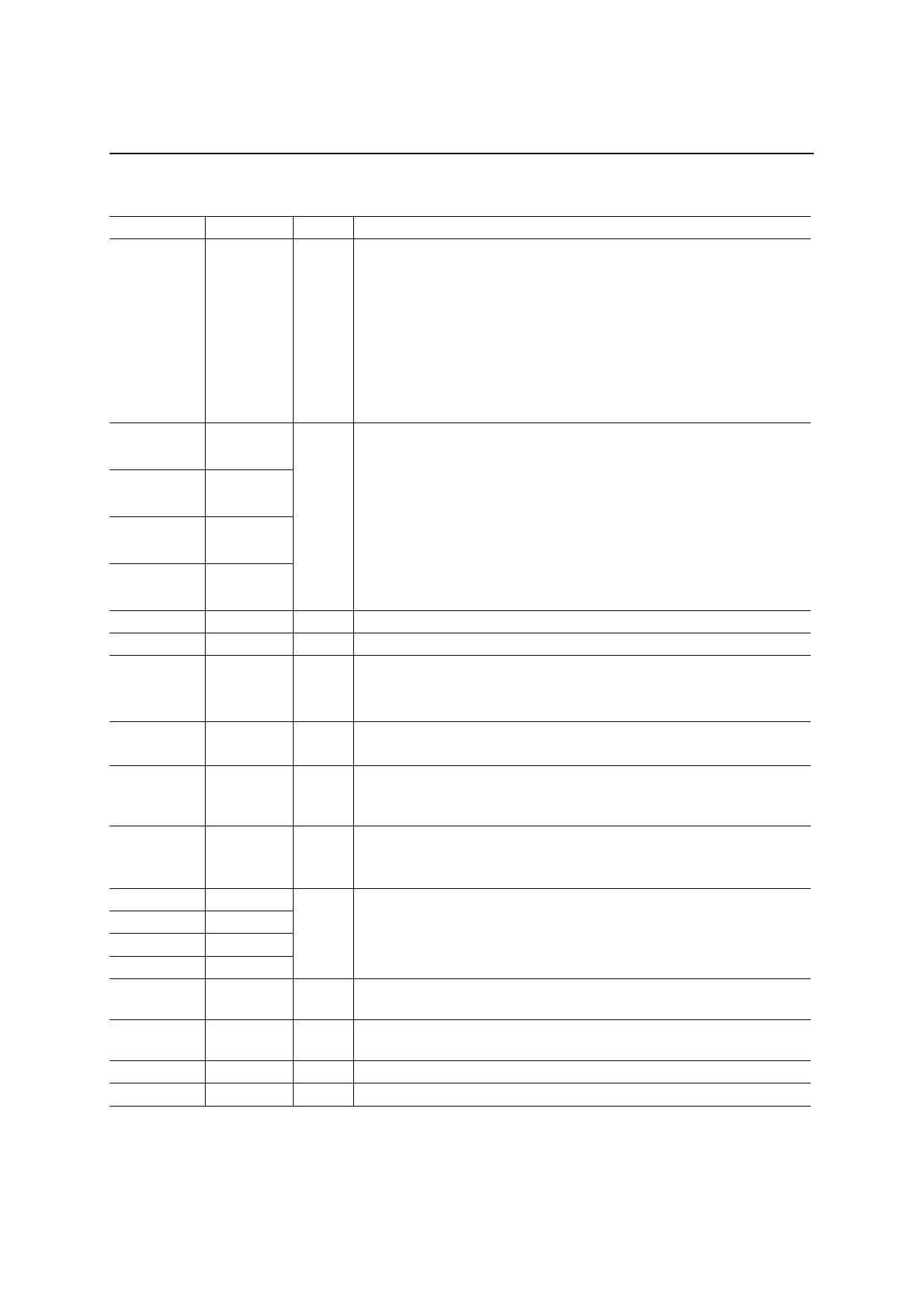
OKI Semiconductor
FEDL9810BFULL-03
MSM9810B
Pin
25
24
23
22
21
4
5
11
12
29
19
9
10
13
3
6
7, 48
2
1, 32
Symbol
D4/UD
D3/SR3
D2/SR2
D1/SR1
D0/SR0
LDAO
RDAO
XT
XT
RESET
NCR/BUSY
TEST1
TEST2
TEST3
TEST4
AVDD
DVDD
AGND
DGND
Type
I/O
I/O
O
O
I
O
I
I
I
—
—
—
—
Description
Data bus pin for CPU interface when parallel input interface is selected.
When WR is “L”, this pin serves as data input pin.
When RD is “L”, this pin serves as channel status output pin.
When serial input interface is selected, this pin serves as channel status
select pin.
When UD is “H”, channels 8 thru 5 are output to SR3 thru SR0,
respectively.
When UD is “L”, channels 4 thru 1 are output to SR3 thru SR0,
respectively.
Data bus pin for CPU interface when parallel input interface is selected.
When WR is “L”, this pin serves as data input pin.
When RD is “L”, this pin serves as channel status output pin.
When serial input interface is selected, this pin serves as channel status
output pin.
When UD is “H”, channels 8 thru 5 are output to SR3 thru SR0,
respectively.
When UD is “L”, channels 4 thru 1 are output to SR3 thru SR0,
respectively.
LEFT side analog output pin.
RIGHT side analog output pin.
Crystal or ceramic oscillator connection pin.
A feedback resistor of about 1MΩ is connected between XT and XT.
When external clocks are used, enter external clocks into this pin.
Crystal or ceramic oscillator connection pin.
When external clocks are used, leave this pin open.
When this pin is “L” level, the LSI is initialized. At that time, oscillation
stops and D/A outputs go to GND level. A pull-up resistor is internally
connected to this pin.
Channel status select pin.
When this pin is “H”, NCR signal is output. When it is “L”, BUSY signal is
output.
Pins for LSI testing. Apply “L” level to these pins.
Analog power supply pin. A bypass capacitor of 01 µF or more should
be connected between the AGND pin and the AVDD pin.
Digital power supply pin. A bypass capacitor of 0.1 µF or more should be
connected between the DGND pin and the DVDD pin.
Analog GND pin.
Digital GND pin.
5/45
Share Link: 