APA3160A View Datasheet(PDF) - Anpec Electronics
Part Name
Description
Manufacturer
APA3160A Datasheet PDF : 38 Pages
| |||
APA3160A
Function Description (Cont.)
Single-Byte Transfers
The serial control interface supports single-byte and multiple-byte (R/W) operations for sub-addresses 0x00 to 0xFF.
Supplying a sub-address for each sub-address transaction is referred to as random I2C addressing. The APA3160A
also supports sequential I2C addressing. For write transactions, if a sub-address is issued and followed by data for
that sub-address and the 15 sub-addresses that follow, a sequential I2C write transaction has taken place, and the
data for all 16 sub-addresses is successfully received by the APA3160A. For I2C sequential write transactions, the
sub-address then serves as the start address, and the amount of data subsequently transmitted, before a stop or
start is transmitted, determines how many sub-addresses are written. As was true for random addressing, sequen-
tial addressing requires that a complete set of data be transmitted. If only a partial set of data is written to the last sub-
address, the data for the last sub-address is discarded. However, if all other data written is accepted, only the
incomplete data is discarded.
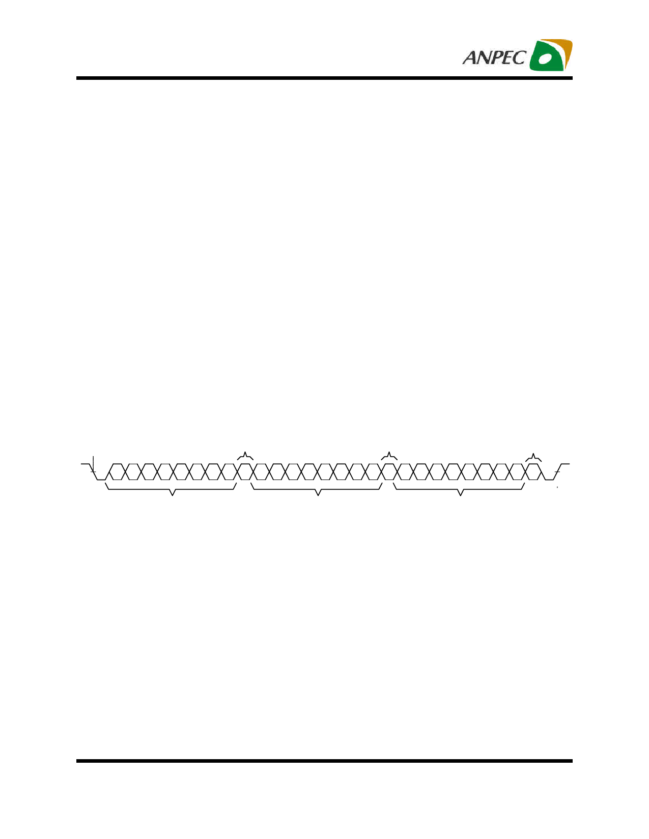
Single-Byte Write
As shown in Figure 11, a single-byte data write transfer begins with the master device transmitting a start condition
followed by the I2C device address and the R/W bit. The R/W bit determines the direction of the data transfer. For a write
data transfer, the R/W bit will be a 0. After receiving the correct I2C device address and the R/W bit, the DAP responds
with an acknowledge bit. And then, the master transmits the address byte or bytes corresponding to the APA3160A
internal memory address being accessed. After receiving the address byte, the APA3160A responds with an acknowl-
edge bit again. Next, the master device transmits the data byte to be written to the memory address being accessed.
After receiving the data byte, the APA3160A responds again with an acknowledge bit. Finally, the master device
transmits a stop condition to complete the single-byte data write transfer.
Start
Condition
Acknowledge
Acknowledge
Acknowledge
A6 A5 A4 A3 A2 A1 A0 R/W ACK A7 A6 A5 A4 A3 A2 A1 A0 ACK D7 D6 D5 D4 D3 D2 D1 D0 ACK
I2C Device Address
and Read/ Write Bit
Sub-address
Data Byte
Stop
Condition
Figure 11. Single-Byte Write Transfer
Copyright © ANPEC Electronics Corp.
16
Rev. A.6 - Jan., 2013
www.anpec.com.tw
Share Link: 