ADSP-21160M(Rev0) View Datasheet(PDF) - Analog Devices
Part Name
Description
Manufacturer
ADSP-21160M Datasheet PDF : 52 Pages
| |||
ADSP-21160M
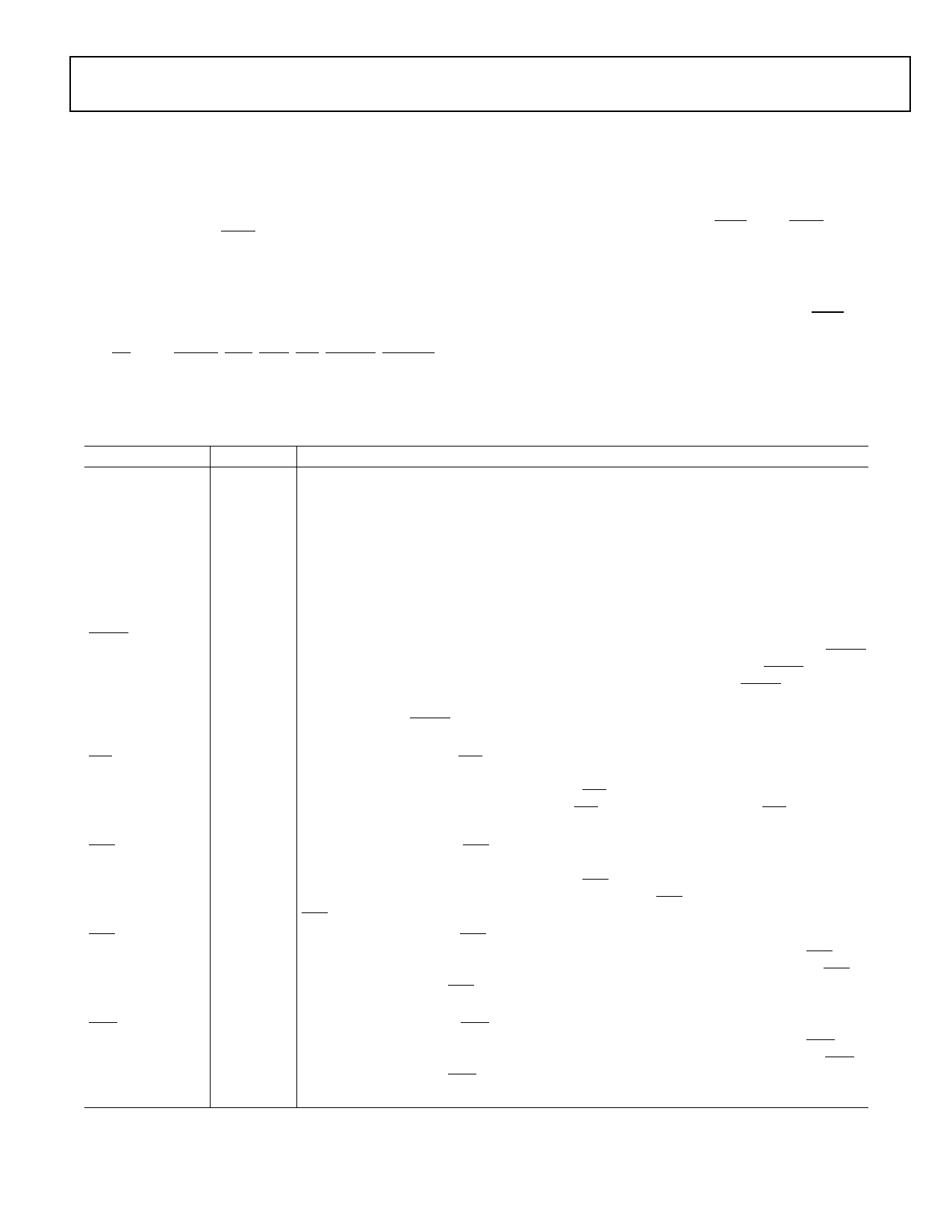
Table 2. Pin Function Descriptions (Continued)
Pin
DMAG2
BR6ã1
Type
O/T
I/O/S
RPBA
I/S
PA
I/O/T
DTx
DRx
TCLKx
RCLKx
TFSx
RFSx
LxDAT7ã0
LxCLK
LxACK
EBOOT
LBOOT
BMS
CLKIN
O
I
I/O
I/O
I/O
I/O
I/O
I/O
I/O
I
I
I/O/T
I
CLK_CFG3ã0 I
CLKOUT
O/T
RESET
I/A
Function
DMA Grant 2 (DMA Channel 12). Asserted by ADSP-21160M to indicate that the
requested DMA starts on the next cycle. Driven by bus master only.
Multiprocessing Bus Requests. Used by multiprocessing ADSP-21160Ms to arbitrate
for bus mastership. An ADSP-21160M only drives its own BRx line (corresponding to
the value of its ID2ã0 inputs) and monitors all others. In a multiprocessor system with
less than six ADSP-21160Ms, the unused BRx pins should be pulled high; the
processorãs own BRx line must not be pulled high or low because it is an output.
Rotating Priority Bus Arbitration Select. When RPBA is high, rotating priority for
multiprocessor bus arbitration is selected. When RPBA is low, fixed priority is selected.
This signal is a system configuration selection which must be set to the same value on
every ADSP-21160M. If the value of RPBA is changed during system operation, it must
be changed in the same CLKIN cycle on every ADSP-21160M.
Priority Access. Asserting its PA pin allows an ADSP-21160M bus slave to interrupt
background DMA transfers and gain access to the external bus. PA is connected to all
ADSP-21160Ms in the system. If access priority is not required in a system, the PA pin
should be left unconnected.
Data Transmit (Serial Ports 0, 1). Each DT pin has a 50 kãÎ internal pull-up resistor.
Data Receive (Serial Ports 0, 1). Each DR pin has a 50 kãÎ internal pull-up resistor.
Transmit Clock (Serial Ports 0, 1). Each TCLK pin has a 50 kãÎ internal
pull-up resistor.
Receive Clock (Serial Ports 0, 1). Each RCLK pin has a 50 kãÎ internal pull-up resistor.
Transmit Frame Sync (Serial Ports 0, 1).
Receive Frame Sync (Serial Ports 0, 1).
Link Port Data (Link Ports 0ã5). Each LxDAT pin has a 50 kãÎ internal pull-down
resistor that is enabled or disabled by the LPDRD bit of the LCTL0ã1 register.
Link Port Clock (Link Ports 0ã5). Each LxCLK pin has a 50 kãÎ internal pull-down
resistor that is enabled or disabled by the LPDRD bit of the LCTL0ã1 register.
Link Port Acknowledge (Link Ports 0ã5). Each LxACK pin has a 50 kãÎ internal
pull-down resistor that is enabled or disabled by the LPDRD bit of the LCOM register.
EPROM Boot Select. For a description of how this pin operates, see Table 3. This
signal is a system configuration selection that should be hardwired.
Link Boot. For a description of how this pin operates, see Table 3. This signal is a
system configuration selection that should be hardwired.
Boot Memory Select. Serves as an output or input as selected with the EBOOT and
LBOOT pins; see Table 3. This input is a system configuration selection that should
be hardwired.
Local Clock In. CLKIN is the ADSP-21160M clock input. The ADSP-21160M
external port cycles at the frequency of CLKIN. The instruction cycle rate is a multiple
of the CLKIN frequency; it is programmable at power-up. CLKIN may not be halted,
changed, or operated below the specified frequency.
Core/CLKIN Ratio Control. ADSP-21160M core clock (instruction cycle) rate is equal
to n Ä CLKIN where n is user-selectable to 2, 3, or 4, using the CLK_CFG3ã0 inputs.
For clock configuration definitions, see the RESET & CLKIN section of the System
Design chapter of the ADSP-21160 SHARC DSP Hardware Reference manual.
Local Clock Out. CLKOUT is driven at the CLKIN frequency by the current bus
master. This output is three-stated when the ADSP-21160M is not the bus master, or
when the host controls the bus (HBG asserted). A keeper latch on the DSPãs CLKOUT
pin maintains the output at the level it was last driven (only enabled on the
ADSP-21160M with ID2ã0 = 00x).
Processor Reset. Resets the ADSP-21160M to a known state and begins execution at
the program memory location specified by the hardware reset vector address. The
RESET input must be asserted (low) at power-up.
REV. 0
ã11ã
Share Link: 