ADSP-21160NCBZ-100(RevD) View Datasheet(PDF) - Analog Devices
Part Name
Description
Manufacturer
ADSP-21160NCBZ-100 Datasheet PDF : 58 Pages
| |||
ADSP-21160M/ADSP-21160N
PIN FUNCTION DESCRIPTIONS
ADSP-21160x pin definitions are listed below. Inputs identified
as synchronous (S) must meet timing requirements with respect
to CLKIN (or with respect to TCK for TMS, TDI). Inputs iden-
tified as asynchronous (A) can be asserted asynchronously to
CLKIN (or to TCK for TRST).
Tie or pull unused inputs to VDD or GND, except for the
following:
• ADDR31–0, DATA63–0, PAGE, BRST, CLKOUT (ID2–0
= 00x) (Note: These pins have a logic-level hold circuit
enabled on the ADSP-21160x DSP with ID2–0 = 00x.)
• PA, ACK, MS3–0, RDx, WRx, CIF, DMARx, DMAGx
(ID2–0 = 00x) (Note: These pins have a pull-up enabled on
the ADSP-21160x with ID2–0 = 00x.)
• LxCLK, LxACK, LxDAT7–0 (LxPDRDE = 0) (Note: See
Link Port Buffer Control Register Bit definitions in the
ADSP-21160 SHARC DSP Hardware Reference.)
• DTx, DRx, TCLKx, RCLKx, EMU, TMS, TRST, TDI
(Note: These pins have a pull-up.)
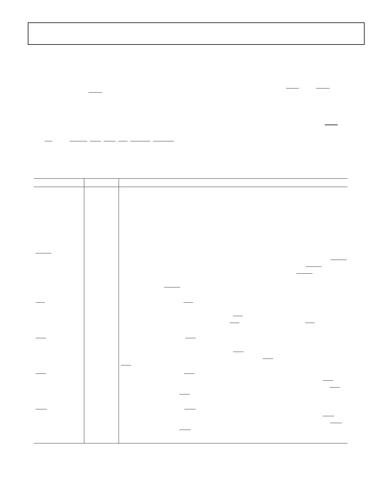
The following symbols appear in the Type column of Table 3:
A = Asynchronous, G = Ground, I = Input, O = Output,
P = Power Supply, S = Synchronous, (A/D) = Active Drive,
(O/D) = Open Drain, and T = Three-State (when SBTS is
asserted, or when the ADSP-21160x is a bus slave).
Table 3. Pin Function Descriptions
Pin
ADDR31–0
DATA63–0
MS3–0
RDL
RDH
WRL
WRH
Type
I/O/T
I/O/T
O/T
I/O/T
I/O/T
I/O/T
I/O/T
Function
External Bus Address. The ADSP-21160x outputs addresses for external memory and peripherals
on these pins. In a multiprocessor system, the bus master outputs addresses for read/writes of the
internal memory or IOP registers of other ADSP-21160x DSPs. The ADSP-21160x inputs addresses
when a host processor or multiprocessing bus master is reading or writing its internal memory or
IOP registers. A keeper latch on the DSP’s ADDR31–0 pins maintains the input at the level it was
last driven (only enabled on the processor with ID2–0 = 00x).
External Bus Data. The ADSP-21160x inputs and outputs data and instructions on these pins. Pull-
up resistors on unused DATA pins are not necessary. A keeper latch on the DSP’s DATA63-0 pins
maintains the input at the level it was last driven (only enabled on the processor with ID2–0 = 00x).
Memory Select Lines. These outputs are asserted (low) as chip selects for the corresponding banks
of external memory. Memory bank size must be defined in the SYSCON control register. The MS3–0
outputs are decoded memory address lines. In asynchronous access mode, the MS3–0 outputs
transition with the other address outputs. In synchronous access modes, the MS3–0 outputs assert
with the other address lines; however, they deassert after the first CLKIN cycle in which ACK is
sampled asserted. MS3–0 has a 20 k internal pull-up resistor that is enabled on the ADSP-21160x
with ID2–0 = 00x.
Memory Read Low Strobe. RDL is asserted whenever ADSP-21160x reads from the low word of
external memory or from the internal memory of other ADSP-21160x DSPs. External devices,
including other ADSP-21160x DSPs, must assert RDL for reading from the low word of processor
internal memory. In a multiprocessing system, RDL is driven by the bus master. RDL has a 20 k
internal pull-up resistor that is enabled on the processor with ID2–0 = 00x.
Memory Read High Strobe. RDH is asserted whenever ADSP-21160x reads from the high word of
external memory or from the internal memory of other ADSP-21160x DSPs. External devices,
including other ADSP-21160x DSPs, must assert RDH for reading from the high word of
ADSP-21160x internal memory. In a multiprocessing system, RDH is driven by the bus master.
RDH has a 20 k internal pull-up resistor that is enabled on the processor with ID2–0 = 00x.
Memory Write Low Strobe. WRL is asserted when ADSP-21160x writes to the low word of external
memory or internal memory of other ADSP-21160x DSPs. External devices must assert WRL for
writing to ADSP-21160x DSP’s low word of internal memory. In a multiprocessing system, WRL is
driven by the bus master. WRL has a 20 k internal pull-up resistor that is enabled on the processor
with ID2–0 = 00x.
Memory Write High Strobe. WRH is asserted when ADSP-21160x writes to the high word of external
memory or internal memory of other ADSP-21160x DSPs. External devices must assert WRH for
writing to ADSP-21160x DSP’s high word of internal memory. In a multiprocessing system, WRH is
driven by the bus master. WRH has a 20 k internal pull-up resistor that is enabled on the processor
with ID2–0 = 00x.
Rev. D | Page 11 of 58 | September 2015
Share Link: 