MPC8349VVAGDB View Datasheet(PDF) - Freescale Semiconductor
Part Name
Description
Manufacturer
MPC8349VVAGDB
Freescale Semiconductor

MPC8349VVAGDB Datasheet PDF : 87 Pages
| |||
Clock Input Timing
4 Clock Input Timing
This section provides the clock input DC and AC electrical characteristics for the device.
4.1 DC Electrical Characteristics
Table 6 provides the clock input (CLKIN/PCI_SYNC_IN) DC timing specifications for the MPC8349EA.
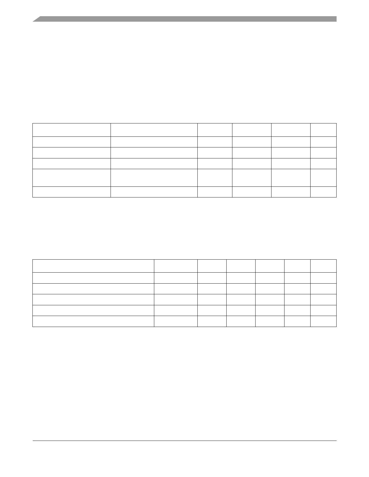
Table 6. CLKIN DC Timing Specifications
Parameter
Input high voltage
Input low voltage
CLKIN input current
PCI_SYNC_IN input current
PCI_SYNC_IN input current
Condition
—
—
0 V ≤ VIN ≤ OVDD
0 V ≤ VIN ≤ 0.5 V or
OVDD – 0.5 V ≤ VIN ≤ OVDD
0.5 V ≤VIN ≤ OVDD – 0.5 V
Symbol
VIH
VIL
IIN
IIN
IIN
Min
Max
Unit
2.7
–0.3
OVDD + 0.3
V
0.4
V
—
±10
μA
—
±10
μA
—
±50
μA
4.2 AC Electrical Characteristics
The primary clock source for the MPC8349EA can be one of two inputs, CLKIN or PCI_CLK, depending
on whether the device is configured in PCI host or PCI agent mode. Table 7 provides the clock input
(CLKIN/PCI_CLK) AC timing specifications for the device.
Table 7. CLKIN AC Timing Specifications
Parameter/Condition
Symbol
Min
Typical
Max
Unit Notes
CLKIN/PCI_CLK frequency
CLKIN/PCI_CLK cycle time
CLKIN/PCI_CLK rise and fall time
CLKIN/PCI_CLK duty cycle
CLKIN/PCI_CLK jitter
fCLKIN
—
tCLKIN
15
tKH, tKL
0.6
tKHK/tCLKIN
40
—
—
—
66
MHz
1, 6
—
—
ns
—
1.0
2.3
ns
2
—
60
%
3
—
±150
ps
4, 5
Notes:
1. Caution: The system, core, USB, security, and TSEC must not exceed their respective maximum or minimum operating
frequencies.
2. Rise and fall times for CLKIN/PCI_CLK are measured at 0.4 and 2.7 V.
3. Timing is guaranteed by design and characterization.
4. This represents the total input jitter—short term and long term—and is guaranteed by design.
5. The CLKIN/PCI_CLK driver’s closed loop jitter bandwidth should be < 500 kHz at –20 dB. The bandwidth must be set low to
allow cascade-connected PLL-based devices to track CLKIN drivers with the specified jitter.
6. Spread spectrum clocking is allowed with 1% input frequency down-spread at maximum 50 KHz modulation rate regardless
of input frequency.
MPC8349EA PowerQUICC II Pro Integrated Host Processor Hardware Specifications, Rev. 13
12
Freescale Semiconductor
Share Link: