MC141535 View Datasheet(PDF) - Motorola => Freescale
Part Name
Description
Manufacturer
MC141535 Datasheet PDF : 26 Pages
| |||
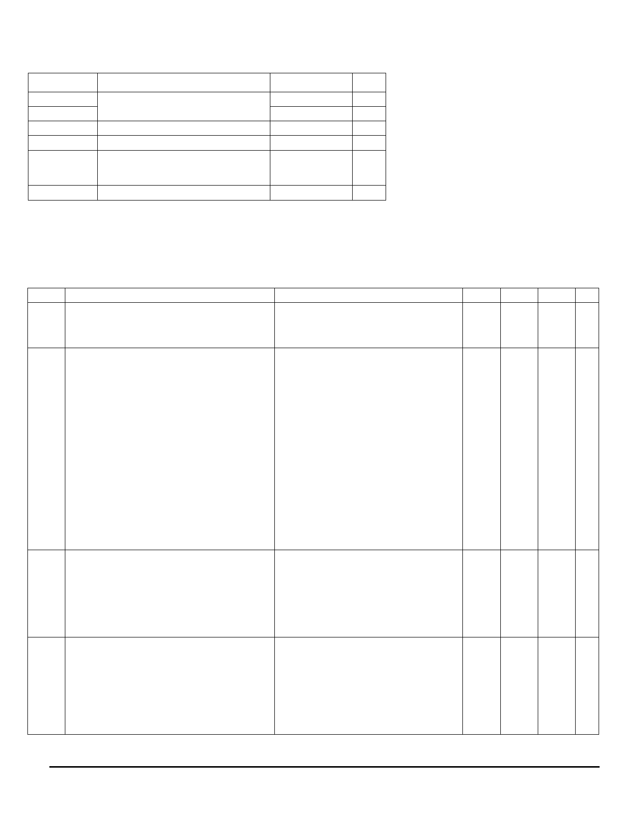
MAXIMUM RATINGS* (Voltages Referenced to VSS, TA=25˚C)
Symbol
Parameter
Value
Unit
AVDD,DVDD
VCC
Vin
I
TA1
TA2
Tstg
Supply Voltage
-0.3 to +4.0
V
VSS-0.3 to VSS+10.5 V
Input Voltage
VSS-0.3 to VDD+0.3
V
Current Drain Per Pin Excluding VDD and VSS
25
mA
Operating Temperature
For Using Internal Oscillator
For Using External Oscillator
-25 to +85
˚C
-30 to +85
˚C
Storage Teperature Range
-65 to +150
˚C
This device contains circuitry to protect the inputs
against damage due to high static voltages or elec-
tric fields; however, it is advised that normal precau-
tions to be taken to avoid application of any voltage
higher than maximum rated voltages to this high
impedance circuit. For proper operation it is recom-
mended that Vin and Vout be constrained to the
range VSS < or = (Vin or Vout) < or = VDD. Reliability
of operation is enhanced if unused input are con-
nected to an appropriate logic voltage level (e.g.,
either VSS or VDD). Unused outputs must be left
open. This device may be light sensitive. Caution
should be taken to avoid exposure of this device to
any light source during normal operation. This
device is not radiation protected.
* Maximum Ratings are those values beyond which damage to the device may occur. Functional
operation should be restricted to the limits in the Electrical Characteristics tables or Pin Descrip-
tion section.
VSS = AVSS = DVSS (DVSS = VSS of Digital circuit, AVSS = VSS of Analogue Circuit)
VDD = AVDD = DVDD (DVDD = VDD of Digital circuit, AVDD = VDD of Analogue Circuit)
ELECTRICAL CHARACTERISTICS (Voltage Referenced to VSS, TA=25˚C)
Symbol
Parameter
Test Condition
Min
Typ
Max Unit
DVDD
AVDD
Supply voltage (Absolute value Referenced to VSS)
Operating Range of Logic Circuit Supply DVDD
Operating Range of Voltage Generator Circuit
Supply AVDD
2.4
3.0
3.5
V
2.4
-
3.5
V
Supply Current (Measure with VDD fixed at 3.0V)
I AC
Access Mode Supply Current Drain from Pin AVDD Internal DC/DC Converter On, Display On, Tripler 0
and DVDD.
Enable, R/W Accessing, Tcyc=1MHz, Osc. Freq.
=38.4kHz, 1/17 Duty Cycle,1/7 Bias.
IDP1
Display Mode Supply Current Drain from Pin AVDD Internal DC/DC Converter On, Display On, Nor- 0
and DVDD.
mal Display Mode, Tripler Enable, R/W Halt, Osc.
Freq.=38.4kHz.
IDP2
Display Mode Supply Current Drain from Pin AVDD Internal DC/DC Converter On, Display On, Nor- 0
and DVDD
mal Display Mode, Tripler Enable, R/W Halt, Osc.
Freq.=38.4kHz. Horizontal Scrolling
IICON
Display Mode Supply Current Drain from Pin AVDD Internal DC/DC Converter On, Display On, Icon -
and DVDD
Display Mode, Tripler Enable, R/W Halt, Osc.
Freq.=38.4kHz.
ISB1
Stand-by Mode Supply Current Drain from Pin
Display Off, Oscillator Disabled, R/W Halt
0
AVDD and DVDD
ISB2
Stand-by Mode Supply Current Drain from Pin
Display Off, Oscillator Enable, R/W Halt, External 0
AVDD and DVDD.
Oscillator and Frequency = 38.4kHz.
ISB3
Stand-by Mode Supply Current Drain from Pin
Display Off, Oscillator Enable, R/W Halt, Internal 0
AVDD and DVDD.
Oscillator and Frequency = 38.4kHz.
200
300 µA
70
100 µA
78
110 µA
15
30 µA
300
500 nA
2.5
5
µA
5
7
µA
VLCD Voltage
VCC1
LCD Driving Voltage Generator Output Voltage at Display On, Internal DC/DC Converter Enabled, -
Pin VCC.
Tripler Enable, Osc. Freq. = 38.4kHz, Regulator
Enabled, Divider Enabled
3*AVDD 10.5 V
VCC2
LCD Driving Voltage Generator Output Voltage at Display On, Internal DC/DC Converter Enabled, -
Pin VCC.
Doubler Enable, Osc. Freq. = 38.4kHz, Regulator
Enabled, Divider Enabled
2*AVDD 10.5 V
VLCD
LCD Driving Voltage input at pin VCC.
Internal DC/DC Converter Disabled.
AVDD
-
10.5 V
VOH1
VOL1
VR1
VR2
VR3
∆VR
Output Voltage
Output High Voltage at Pins D0-D7, Annun0-3, BP
and OSC2.
Output Low Voltage at Pins D0-D7, Annun0-3, BP
and OSC2.
LCD Driving Voltage Source at Pin VR
LCD Driving Voltage Source at Pin VR
Delta of VR Voltage Drop
Variation of VR Input (VDD is fixed)
Iout=100µA
Iout=100µA
Regulator Enabled
Regulator Disabled
Regulator Enabled, Iout=50µA
Regulator Enabled
0.9*VDD
-
VDD
V
0
-
0.1*VDD V
0
-
VCC-0.5 V
-
0
-
V
0
-
VCC V
-
±1
±2.5 %
MC141535
3–76
MOTOROLA
Share Link: 