MC141539 View Datasheet(PDF) - Motorola => Freescale
Part Name
Description
Manufacturer
MC141539 Datasheet PDF : 29 Pages
| |||
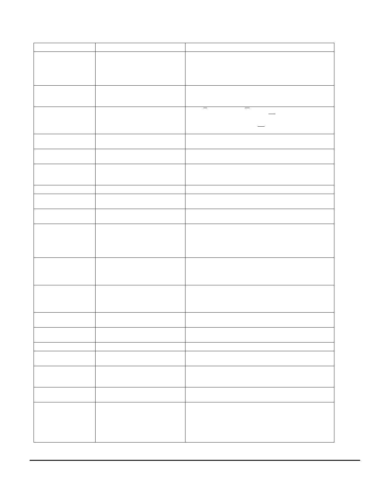
COMMAND TABLE
Bit Pattern
000000X1X0
0001X3X2X1X0
0001X3X2X1X0
0010000X0
0010001X0
0010010X0
0010011X0
0010100X0
0010101X0
0010110X0
0010111X0
0011000X0
0011001X0
0011010X0
0011011X0
0011100X0
0011101X0
010X4X3X2X1X0
01100A1A0X0
Command
Set GDDRAM Page Address
Set Contrast Level
Read Contrast Value
Set Voltage Doubler / Tripler
Set Column Mapping
Set Row Mapping
Reserved
Set Display On/Off
Set Internal DC/DC Converter On/Off
Set Internal Regulator On/Off
Set Internal Voltage Divider On/Off
Set Internal Contrast Control On/Off
Set Clock Frequency
Save/Restore GDDRAM Column
Address
Master Clear GDDRAM
Set Bias Ratio
Reserved.
Set Vertical Scroll Value
Set Annunciator Control Signals
Comment
Set GDDRAM Page Address using X1X0 as address bits.
X1X0=00 : page 1 (POR)
X1X0=01 : page 2
X1X0=10 : page 3
X1X0=11 : page 4
Set one of the 16 available values to the internal contrast register,
using X3X2X1X0 as data bits. The contrast register is reset to 0000
during POR.
With D/C pin input Low, R/W pin input high, and D7 D6 D5 D4 pins
equal to 0001 at the rising edge of CS, the value of the internal
contrast register will be latched out at D3 D2 D1 D0 pins, i.e.
X3X2X1X0, at the rising edge of CS.
X0=0: Select Voltage Tripler (POR)
X0=1: Select Voltage Doubler
X0=0 : Col0 to Seg0 (POR)
X0=1 : Col0 to Seg119
With duty cycle is 1/32
X0=0 : Row0 to Com0 (POR)
X0=1: Row0 to Com31
X0=0: display off (POR)
X0=1: display on
X0=0: Internal DC/DC Converter off (POR)
X0=1: Internal DC/DC Converter on
X0=0: Internal Regulator off (POR)
X0=1: Internal Regulator on
When the application employs external contrast control, the inter-
nal contrast control, temperature compensation and the Regulator
must be enabled.
X0=0: Internal Voltage Divider off (POR)
X0=1: Internal Voltage Divider on
When an external bias network is preferred, the voltage divider
should be disabled.
X0=0: Internal Contrast Control off (POR)
X0=1: Internal Contrast Control on
Internal contrast circuits can be disabled if external contrast cir-
cuits is preferred.
X0=0 : low frequency (38.4kHz) (POR)
X0=1 : high frequency (50kHz)
X0=0 : restore address
X0=1 : save address
Master clear entire GDDRAM
X0=0: set 1/7 bias (POR)
X0=1: set 1/5 bias
X0=0: normal operation (POR)
X0=1: test mode
(Note: Make sure to set X0=0 during application)
Use X4X3X2X1X0 as number of lines to scroll.
Scroll value = 0 upon POR
A1A0=00: select annunciator 1 (POR)
A1A0=01: select annunciator 2
A1A0=10: select annunciator 3
A1A0=11: select annunciator 4
X0=0: turn selected annunciator off (POR)
X0=1: turn selected annunciator on
MC141539
3–138
MOTOROLA
Share Link: 