SSD1820A View Datasheet(PDF) - Solomon Systech
Part Name
Description
Manufacturer
SSD1820A Datasheet PDF : 43 Pages
| |||
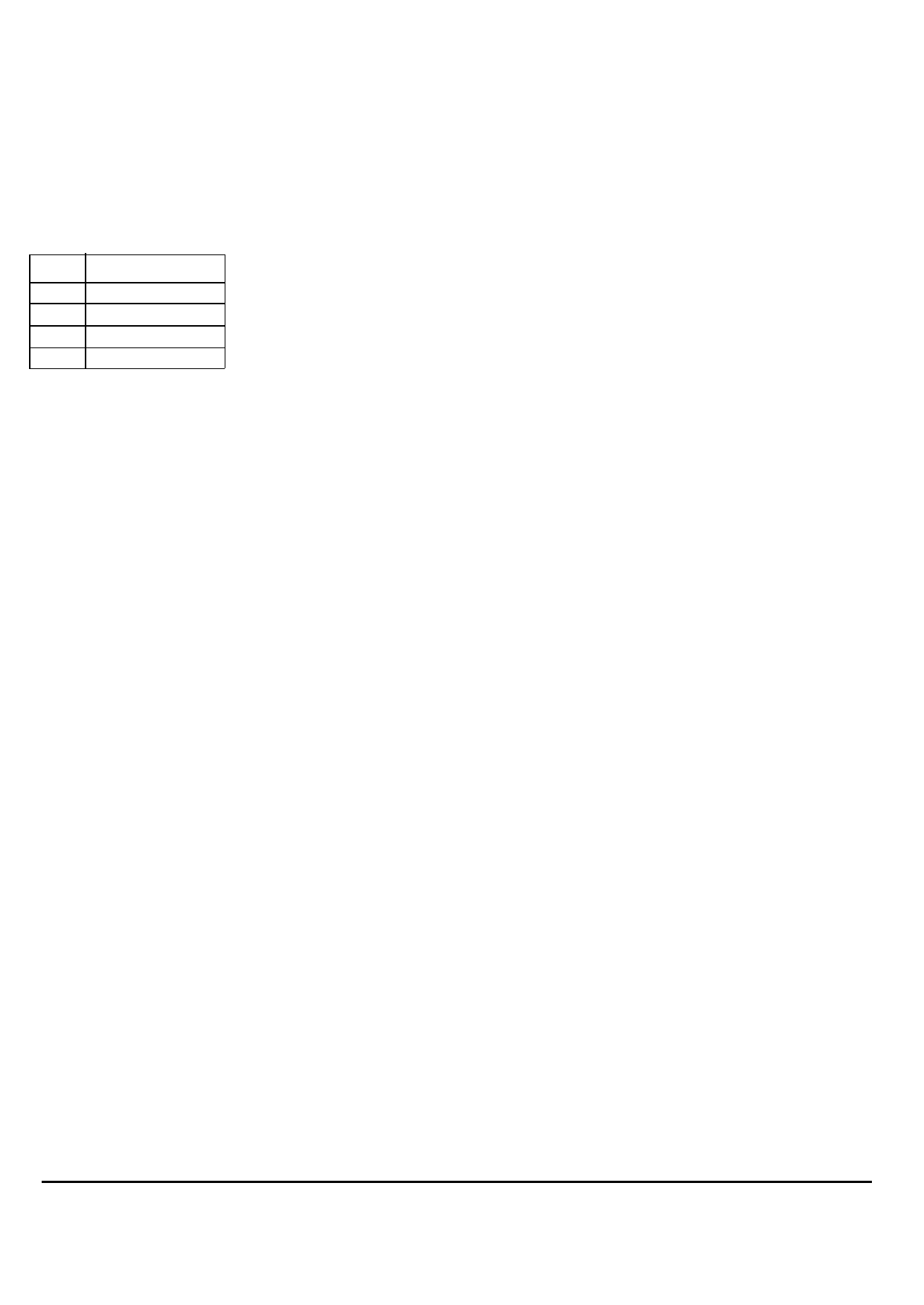
VL5, VL4, VL3 and VL2
LCD driving voltages. They can be supplied externally or gener-
ated by the internal bias divider. They have the following relation-
ship:
VL6 > VL5 > VL4 > VL3 > VL2 > VSS
1:a bias
VL5
(a-1)/a*VL6
VL4
(a-2)/a*VL6
VL3
2/a*VL6
VL2
1/a*VL6
For SSD1820A, a equals to 9 at POR.
For SSD1821, a equal to 10 at POR.
COM0 - COM63/COM79
These pins provide the row driving signal COM0 - COM63/
COM79 to the LCD panel. See Table 1 or 2 about the COM signal
mapping in different multiplex ratio N.
ICONS
This pin is the special icons line COM signal output.
SEG0 - SEG127
These pins provide the LCD column driving signal. Their voltage
level is VSS during sleep mode and standby mode.
CL
This pin is the external clock input for the device which is
enabled by using an extended command. Under normal operation,
this pin should be left opened and internal oscillator will be used
after power on reset.
N/C
These No Connection pins should NOT be connected to any sig-
nal pins nor shorted together. They should be left open.
SOLOMON
REV 1.4 SSD1820A/21
01/03
11
Share Link: 