IS42RM16800E View Datasheet(PDF) - Integrated Silicon Solution
Part Name
Description
Manufacturer
IS42RM16800E Datasheet PDF : 25 Pages
| |||
IS42SM81600E / IS42SM16800E / IS42SM32400E
IS42RM81600E / IS42RM16800E / IS42RM32400E
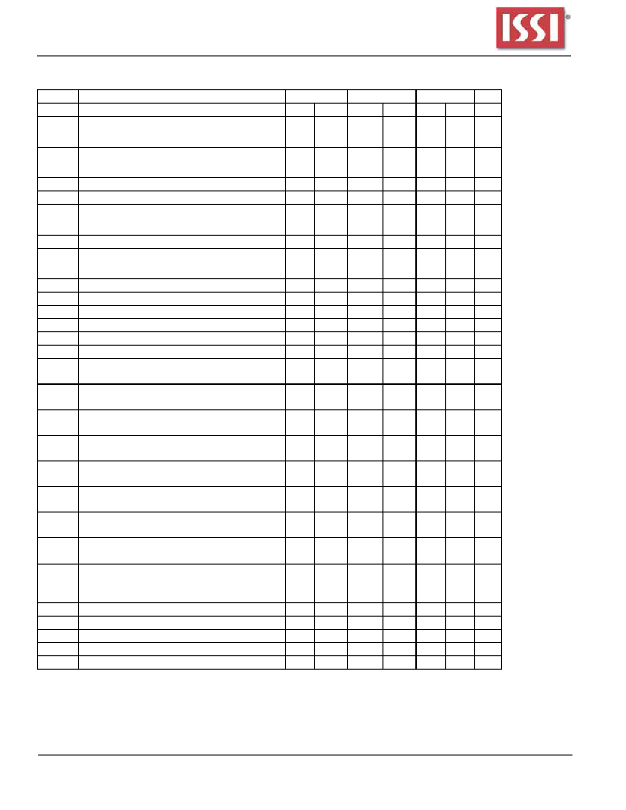
AC ELECTRICAL CHARACTERISTICS (1, 2, 3)
Symbol Parameter
tCK3 Clock Cycle Time
CAS Latency = 3
-64
Min. Max.
6
–
-7
Min. Max.
7
–
-75E
Min. Max. Unit
–
– ns
tCK2
tAC3
Access Time From CLK
CAS Latency = 2 10 –
10
– 7.5 – ns
CAS Latency = 3 – 5.4
–
5.4
–
– ns
tAC2
tCHI
tCL
tOH3
CLK HIGH Level Width
CLK LOW Level Width
Output Data Hold Time
CAS Latency = 2 –
8
–
8
– 5.5 ns
2.5 –
2.5
– 2.5 – ns
2.5 –
2.5
– 2.5 – ns
CAS Latency = 3 2.7 –
2.7
– 2.7 – ns
tOH2
CAS Latency = 2 2.7 –
2.7
– 2.7 – ns
tLZ
Output LOW Impedance Time
0
–
0
–
0
– ns
tHZ
Output HIGH Impedance Time CAS Latency = 3 2.7 5.4 2.7 5.4 2.7 – ns
tDS
tDH
tAS
tAH
tCKS
tCKH
tCS
tCH
tRC
tRAS
tRP
tRCD
tRRD
tDPL
tDAL
tMRD
tDDE
tSRX
tT
tREF
CAS Latency = 2
Input Data Setup Time (2)
Input Data Hold Time (2)
Address Setup Time (2)
Address Hold Time (2)
CKE Setup Time (2)
CKE Hold Time (2)
Command Setup Time (CS,
RAS, CAS, WE, DQM)(2)
Command Hold Time (CS,
RAS, CAS, WE, DQM)(2)
Command Period (REF to REF
/ ACT to ACT)
Command Period (ACT to
PRE)
Command Period (PRE to
ACT)
Active Command to Read/
Write Command Delay Time
Command Period (ACT [0] to
ACT [1])
Input Data to Precharge
Command Delay Time
Input Data to Active/Refresh
Command Delay Time (During
Auto-Precharge)
Mode Register Program Time
Power Down Exit Setup Time
Self-Refresh Exit Time
Transition Time
Refresh Cycle Time (4096)
2.7 8
2.7
8 2.7 5.5
1.5 –
1.5
– 1.5 – ns
1.0 –
1.0
– 1.0 – ns
1.5 –
1.5
– 1.5 – ns
1.0 –
1.0
– 1.0 – ns
1.5 –
1.5
– 1.5 – ns
1.0 –
1.0
– 1.0 – ns
1.5 –
1.5
– 1.5 – ns
1.0 –
1.0
– 1.0 – ns
60 – 67.5 – 67.5 – ns
42 100K 45 100K 45 100K ns
18 –
20
–
15 – ns
18 –
20
–
15 – ns
12 –
14
–
15 – ns
12 –
14
–
15 – ns
30 –
35
–
30 – ns
12 –
14
–
15 – ns
6
–
7
– 7.5 – ns
70 –
70
–
70 – ns
0.3 1.2 0.3 1.2 0.3 1.2 ns
– 64
–
64 – 64 ms
Notes:
1. The power-on sequence must be executed before starting memory operation.
2. Measured with tT = 1 ns. If clock rising time is longer than 1ns, (tR /2 - 0.5) ns should be added to the parameter.
3. The reference level is 1.4V when measuring input signal timing. Rise and fall times are measured between
Vih(min.) and Vil (max).
4. Not available for 2.5V, x32 option.
18
Integrated Silicon Solution, Inc. - www.issi.com
Rev. B
04/15/2011
Share Link: 