STM8S103C2P6 View Datasheet(PDF) - STMicroelectronics
Part Name
Description
Manufacturer
STM8S103C2P6
STMicroelectronics

STM8S103C2P6 Datasheet PDF : 56 Pages
| |||
Product overview
STM8S103xx, STM8S105xx
Write protection (WP)
Write protection of Flash is provided to avoid unintentional overwriting of memory that could
result from a user software malfunction.
There are two levels of write protection. The first level is known as MASS (Memory Access
Security System). MASS is always enabled and protects the main Flash program memory
and option bytes.
To perform In-Application Programming (IAP), this write protection can be removed by
writing a MASS key sequence in a control register. This allows the application to modify the
contents of main program memory or the device option bytes.
A second level of write protection, can be enabled to further protect a specific area of
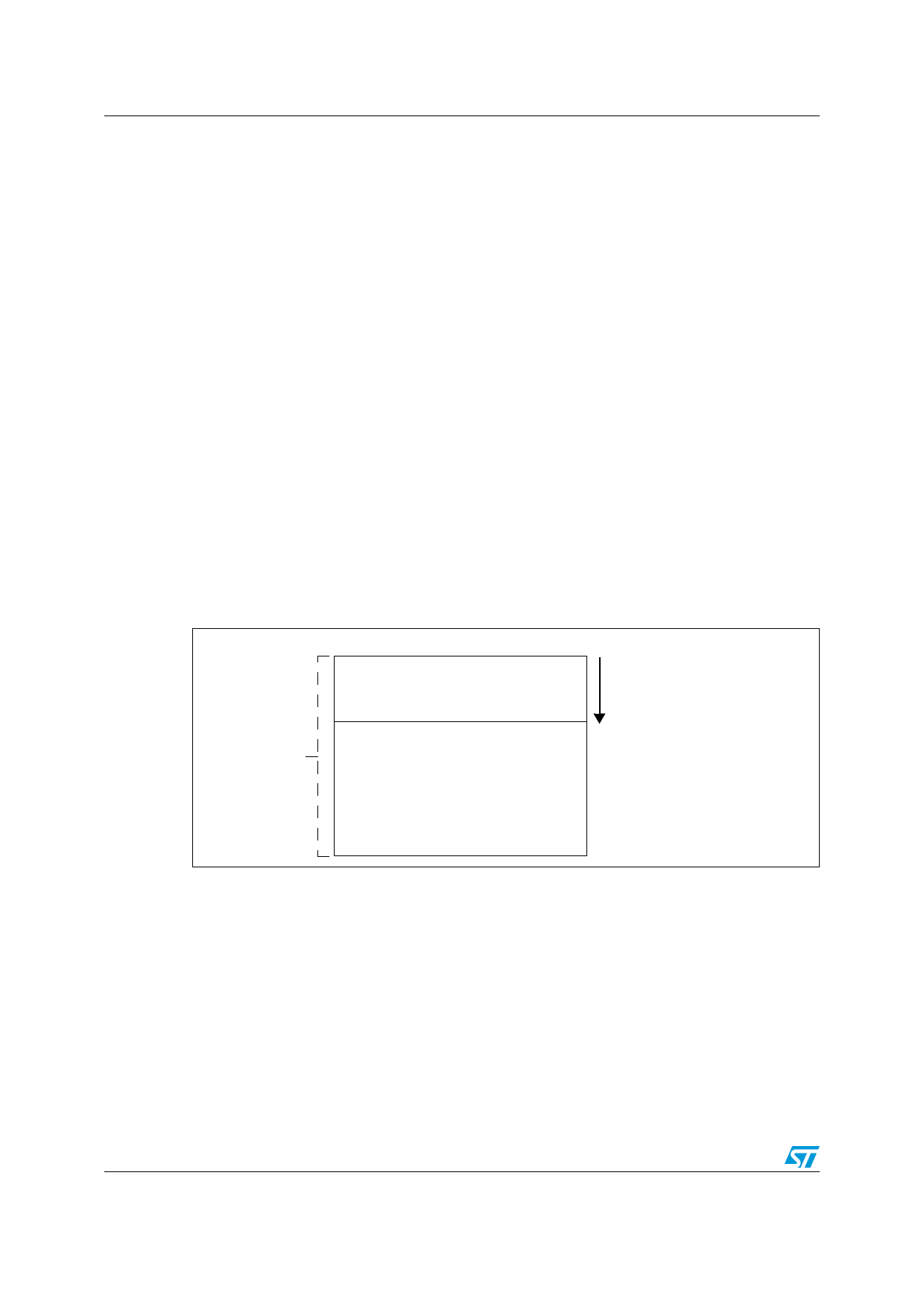
memory known as UBC (user boot code). Refer to Figure 3.
The size of the UBC is programmable through the UBC option byte (Table 8.), in increments
of 1 page, by programming the UBC option byte in ICP mode.
This divides the program memory into two areas:
ŌŚÅ Main program memory: Up to 32 Kbytes minus UBC
ŌŚÅ User-specific boot code (UBC): Configurable up to 32 Kbytes
The UBC area remains write-protected during in-application programming. This means that
the MASS keys do not unlock the UBC area. It protects the memory used to store the boot
program, specific code libraries, reset and interrupt vectors, the reset routine and usually the
IAP and communication routines.
Figure 3. Flash memory organization (STM8S105)
Up to
32 Kbytes
Flash
program
memory
UBC area
Remains write protected during IAP
Program memory area
Write access possible for IAP
Programmable area from 0.5 Kbytes
(2 first pages) up to 32 Kbytes
(1 page steps)
12/56
Share Link: