MT48LC4M32LFFC-10 View Datasheet(PDF) - Micron Technology
Part Name
Description
Manufacturer
MT48LC4M32LFFC-10 Datasheet PDF : 61 Pages
| |||
READs
READ bursts are initiated with a READ command, as
shown in Figure 5.
The starting column and bank addresses are provided
with the READ command, and auto precharge is either
enabled or disabled for that burst access. If auto precharge
is enabled, the row being accessed is precharged at the
completion of the burst. For the generic READ com-
mands used in the following illustrations, auto precharge
is disabled.
During READ bursts, the valid data-out element from
the starting column address will be available following
the CAS latency after the READ command. Each subse-
quent data-out element will be valid by the next positive
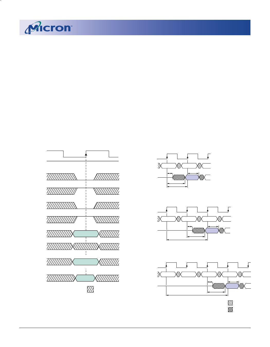
clock edge. Figure 6 shows general timing for each pos-
sible CAS latency setting.
Figure 5
READ Command
CLK
CKE HIGH
CS#
RAS#
CAS#
WE#
A0-A8
A9, A11
A10
BA0,1
COLUMN
ADDRESS
ENABLE AUTO PRECHARGE
DISABLE AUTO PRECHARGE
BANK
ADDRESS
DON’T CARE
ADVANCE
128Mb: x16, x32
MOBILE SDRAM
Upon completion of a burst, assuming no other com-
mands have been initiated, the DQs will go High-Z. A full-
page burst will continue until terminated. (At the end of
the page, it will wrap to column 0 and continue.)
Data from any READ burst may be truncated with a
subsequent READ command, and data from a fixed-length
READ burst may be immediately followed by data from a
READ command. In either case, a continuous flow of data
can be maintained. The first data element from the new
burst follows either the last element of a completed burst
or the last desired data element of a longer burst that is
being truncated. The new READ command should be
issued x cycles before the clock edge at which the last
desired data element is valid, where x equals the CAS
latency minus one.
CLK
COMMAND
DQ
Figure 6
CAS Latency
T0
T1
T2
READ
tLZ
tAC
NOP
tOH
DOUT
CAS Latency = 1
T0
T1
T2
T3
CLK
COMMAND
DQ
READ
NOP
tLZ
tAC
CAS Latency = 2
NOP
tOH
DOUT
CLK
COMMAND
T0
READ
DQ
T1
T2
NOP
NOP
tLZ
tAC
CAS Latency = 3
T3
T4
NOP
tOH
DOUT
DON’T CARE
UNDEFINED
128Mb: x16, x32 Mobile SDRAM
MobileY95W_3V_F.p65 – Rev. F; Pub. 9/02
18
Micron Technology, Inc., reserves the right to change products or specifications without notice.
©2002, Micron Technology, Inc.
Share Link: 