56F8357 View Datasheet(PDF) - Motorola => Freescale
Part Name
Description
Manufacturer
56F8357 Datasheet PDF : 160 Pages
| |||
Freescale Semiconductor, Inc.
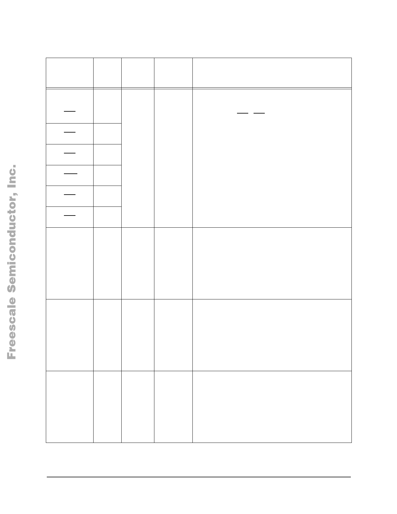
56F8357 Signal Pins
Table 2-2 56F8357 Signal and Package Information for the 160-Pin LQFP
Signal Name Pin No. Type
State
During
Reset
Signal Description
GPIOD0
(CS2)
GPIOD1
(CS3)
GPIOD2
(CS4)
GPIOD3
(CS5)
GPIOD4
(CS6)
GPIOD5
(CS7)
TXD0
(GPIOE0)
RXD0
(GPIOE1)
TXD1
(GPIOD6)
55
Input/
Output
Output
56
57
58
59
60
Input
Port D GPIO — These six GPIO pins can be individually
programmed as input or output pins.
Chip Select — CS2 - CS7 may be programmed within the
EMI module to act as chip selects for specific areas of the
external memory map.
Depending upon the state of the DRV bit in the EMI bus
control register (BCR), A0–A23 and EMI control signals are
tri-stated when the external bus is inactive.
At reset, these pins are configured as GPIO.
To deactivate the internal pull-up resistor, clear the
appropriate GPIO bit in the GPIOD_PUR register.
Example: GPIOD0, clear bit 0 in the GPIOD_PUR register.
4
Output Tri-stated Transmit Data — SCI0 transmit data output
Input/
Output
Input
Port E GPIO — This GPIO pin can be individually
programmed as an input or output pin.
After reset, the default state is SCI output.
To deactivate the internal pull-up resistor, clear bit 0 in the
GPIOE_PUR register.
5
Input
Input
Receive Data — SCI0 receive data input
Input/
Output
Input
Port E GPIO — This GPIO pin can be individually
programmed as an input or output pin.
After reset, the default state is SCI output.
To deactivate the internal pull-up resistor, clear bit 1 in the
GPIOE_PUR register.
49
Output Tri-stated Transmit Data — SCI1 transmit data output
Input/
Output
Input
Port D GPIO — This GPIO pin can be individually
programmed as an input or output pin.
After reset, the default state is SCI output.
To deactivate the internal pull-up resistor, clear bit 6 in the
GPIOD_PUR register.
56F8357 Technical Data
21
Preliminary
For More Information On This Product,
Go to: www.freescale.com
Share Link: 