C8051F912 View Datasheet(PDF) - Silicon Laboratories
Part Name
Description
Manufacturer
C8051F912 Datasheet PDF : 318 Pages
| |||
C8051F91x-C8051F90x
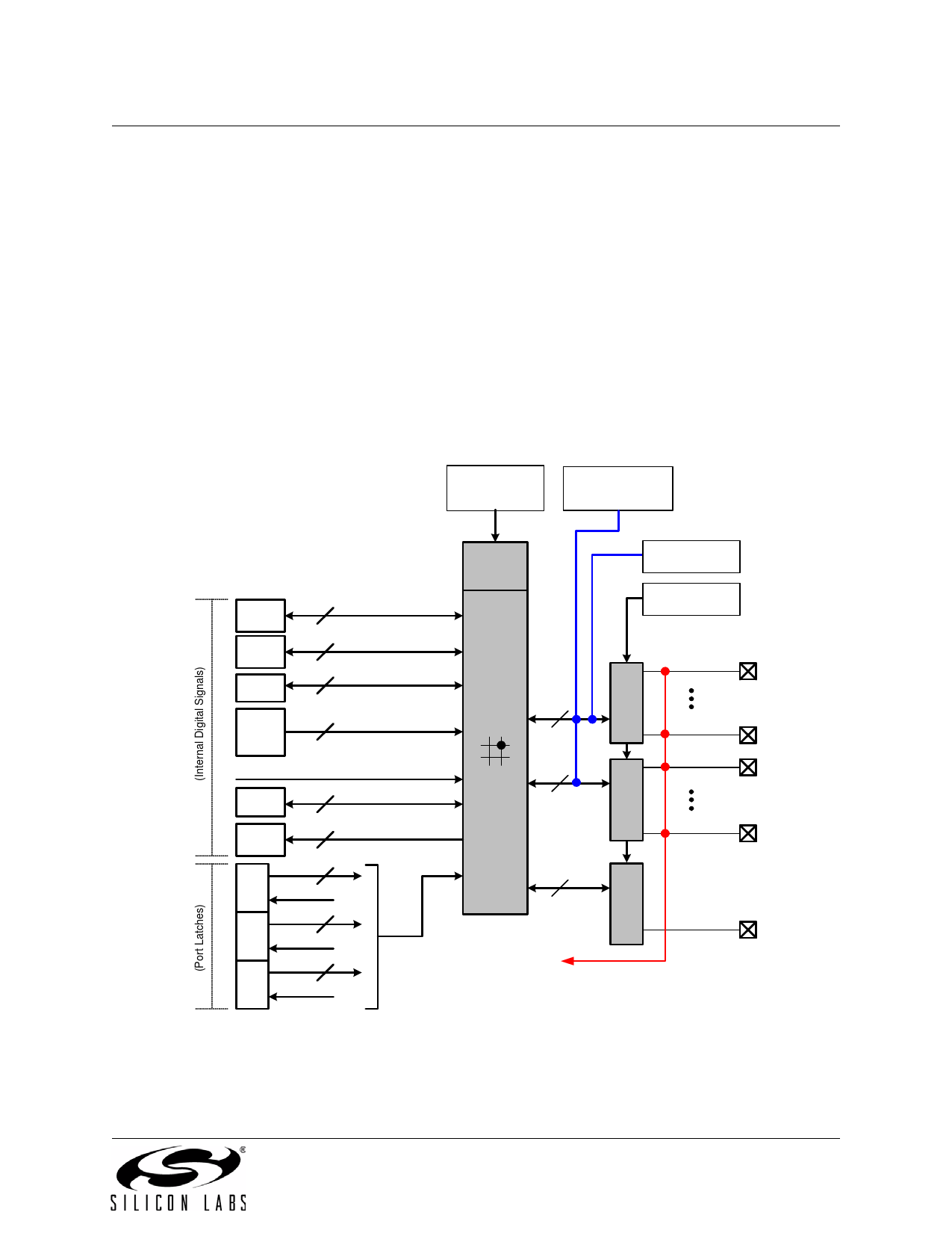
1.2. Port Input/Output
Digital and analog resources are available through 16 I/O pins. Port pins are organized as three byte-wide
ports. Port pins P0.0–P1.6 can be defined as digital or analog I/O. Digital I/O pins can be assigned to one
of the internal digital resources or used as general purpose I/O (GPIO). Analog I/O pins are used by the
internal analog resources. P2.7 can be used as GPIO and is shared with the C2 Interface Data signal
(C2D). See Section “27. C2 Interface” on page 312 for more details.
The designer has complete control over which digital and analog functions are assigned to individual Port
pins, limited only by the number of physical I/O pins. This resource assignment flexibility is achieved
through the use of a Priority Crossbar Decoder. See Section “21.3. Priority Crossbar Decoder” on
page 209 for more information on the Crossbar.
All Port I/Os are 5 V tolerant when used as digital inputs or open-drain outputs. For Port I/Os configured as
push-pull outputs, current is sourced from the VDD/DC+ supply. Port I/Os used for analog functions can
operate up to the VDD/DC+ supply voltage. See Section “21.1. Port I/O Modes of Operation” on page 206
for more information on Port I/O operating modes and the electrical specifications chapter for detailed
electrical specifications.
XBR0, XBR1,
XBR2, PnSKIP
Registers
Port Match
P0MASK, P0MAT
P1MASK, P1MAT
Highest
Priority
Lowest
Priority
2
UART
SPI0
4
SPI1
2
SMBus
CP0
4
CP1
Outputs
SYSCLK
PCA
7
2
T0, T1
8
P0 (P0.0-P0.7)
7
P1 (P1.0-P1.6)
1
P2
(P2.7)
Priority
Decoder
External Interrupts
EX0 and EX1
PnMDOUT,
PnMDIN Registers
Digital
Crossbar
8
P0
I/O
Cells
7
P1
I/O
Cells
1
P2
I/O
Cell
To Analog Peripherals
(ADC0, CP0, and CP1 inputs,
VREF, IREF0, AGND)
P0.0
P0.7
P1.0
P1.6
P2.7
Figure 1.5. Port I/O Functional Block Diagram
Rev. 1.0
21
Share Link: 