MPC8540 View Datasheet(PDF) - Freescale Semiconductor
Part Name
Description
Manufacturer
MPC8540 Datasheet PDF : 104 Pages
| |||
DDR SDRAM
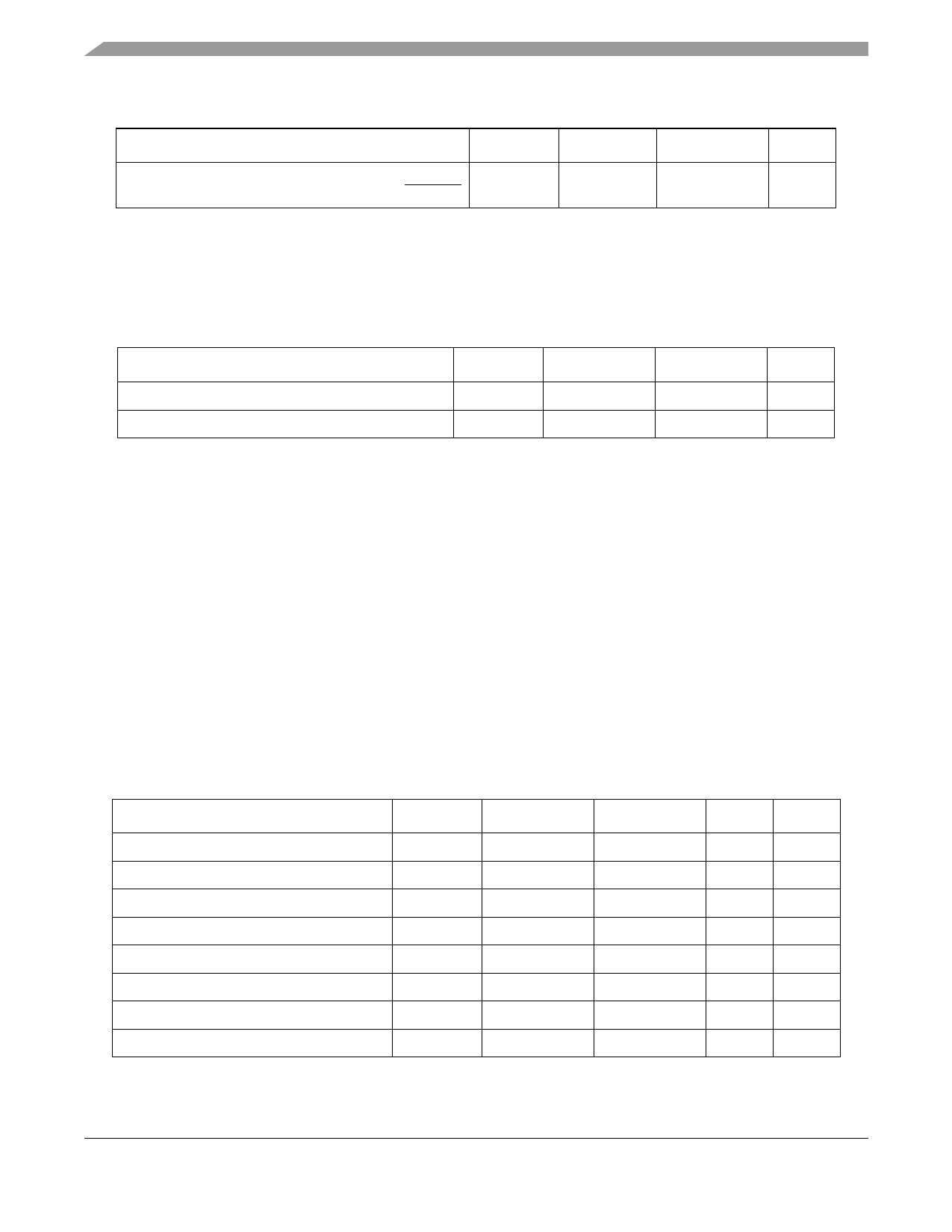
Table 11. RESET Initialization Timing Specifications (continued)
Parameter/Condition
Min
Max
Unit
Notes
Maximum valid-to-high impedance time for actively
—
driven POR configs with respect to negation of HRESET
5
SYSCLKs
1
Notes:
1.SYSCLK is identical to the PCI_CLK signal and is the primary clock input for the MPC8540. See the MPC8540
Integrated Processor Preliminary Reference Manual for more details.
Table 12 provides the PLL and DLL lock times.
Table 12. PLL and DLL Lock Times
Parameter/Condition
Min
Max
Unit
Notes
PLL lock times
—
100
μs
DLL lock times
7680
122,880
CCB Clocks
1, 2
Notes:
1.DLL lock times are a function of the ratio between the output clock and the platform (or CCB) clock. A 2:1 ratio
results in the minimum and an 8:1 ratio results in the maximum.
2. The CCB clock is determined by the SYSCLK × platform PLL ratio.
6 DDR SDRAM
This section describes the DC and AC electrical specifications for the DDR SDRAM interface of the
MPC8540.
6.1 DDR SDRAM DC Electrical Characteristics
Table 13 provides the recommended operating conditions for the DDR SDRAM component(s) of the
MPC8540.
Table 13. DDR SDRAM DC Electrical Characteristics
Parameter/Condition
I/O supply voltage
I/O reference voltage
I/O termination voltage
Input high voltage
Input low voltage
Output leakage current
Output high current (VOUT = 1.95 V)
Output low current (VOUT = 0.35 V)
Symbol
GVDD
MVREF
VTT
VIH
VIL
IOZ
IOH
IOL
Min
2.375
0.49 × GVDD
MVREF – 0.04
MVREF + 0.18
–0.3
–10
–15.2
15.2
Max
2.625
0.51 × GVDD
MVREF + 0.04
GVDD + 0.3
MVREF – 0.18
10
—
—
Unit
V
V
V
V
V
μA
mA
mA
Notes
1
2
3
4
4
5
MPC8540 Integrated Processor Hardware Specifications, Rev. 4
16
Freescale Semiconductor
Share Link: 