TC1321EUA View Datasheet(PDF) - Microchip Technology
Part Name
Description
Manufacturer
TC1321EUA Datasheet PDF : 24 Pages
| |||
TC1321
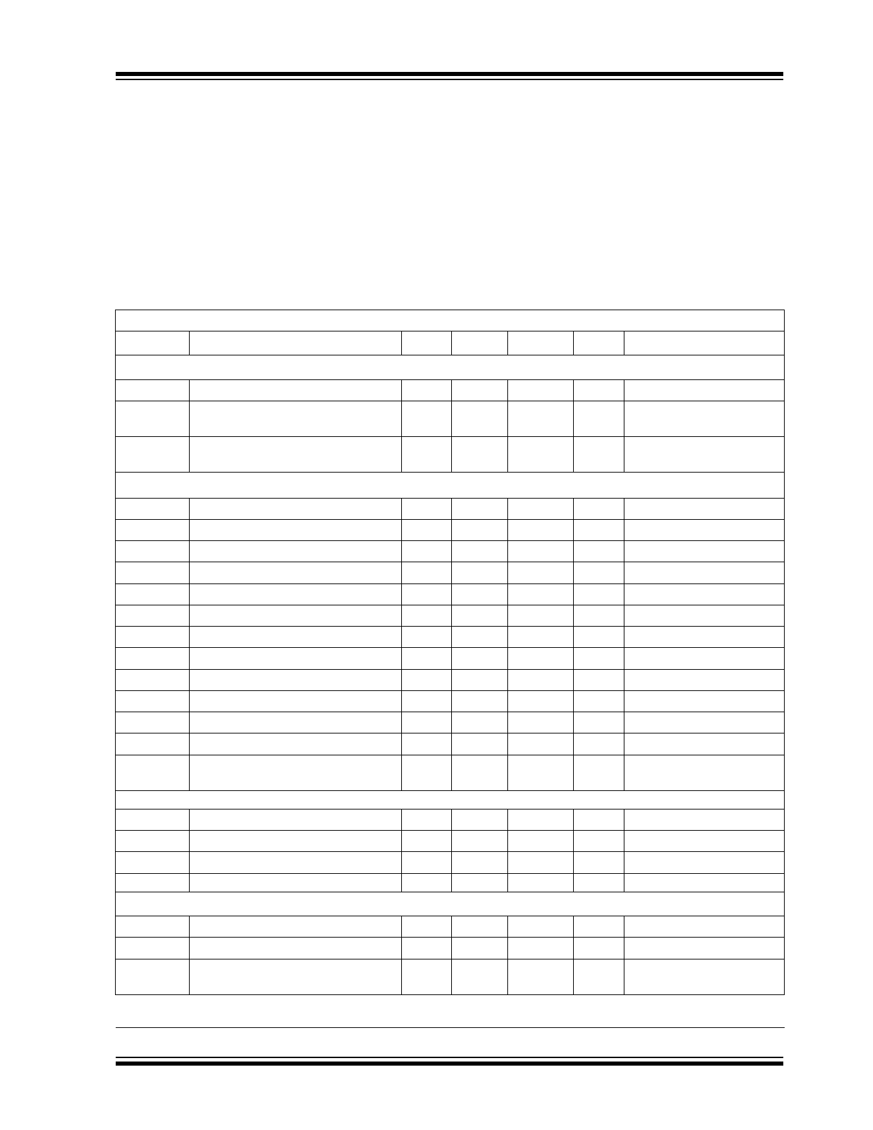
1.0 ELECTRICAL
CHARACTERISTICS
Absolute Maximum Ratings*
Supply Voltage (VDD) ........................................................+6V
Voltage on any Pin ....................(VSS – 0.3V) to (VDD + 0.3V)
Current on any Pin ......................................................±50 mA
Package Thermal Resistance (JA)....................... 330°C C/W
Operating Temperature (TA)................................... See Below
Storage Temperature (TSTG) .........................-65°C to +150°C
ELECTRICAL SPECIFICATIONS
*Stresses above those listed under “Absolute Maximum
Ratings” may cause permanent damage to the device. These
are stress ratings only and functional operation of the device
at these or any other conditions above those indicated in the
operation sections of the specifications is not implied.
Exposure to Absolute Maximum Rating conditions for
extended periods may affect device reliability.
Electrical Characteristics: VDD = 2.7V to 5.5V, -40°C TA +85°C, VREF = 1.2 V unless otherwise noted.
Symbol
Parameter
Min
Typ
Max
Unit
Test Conditions
Power Supply
VDD
Supply Voltage
IDD
Operating Current
IDD-
STANDBY
Standby Supply Current
Static Performance - Analog Section
2.7
—
5.5
V
—
350
500
µA VDD = 5.5V, VREF = 1.2V
Serial Port Inactive (Note 1)
—
0.1
1
µA
VDD = 3.3V
Serial Port Inactive (Note 1)
Resolution
—
—
10
INL
Integral Non-Linearity at FS, TA = +25°C —
—
±4.0
FSE
Full Scale Error
—
—
±3
DNL
Differential Non-Linearity, TA = +25°C
-1
—
+2
VOS
Offset Error at VOUT
—
±0.3
±8
TCVOS
Offset Error Tempco at VOUT
—
10
—
PSRR
Power Supply Rejection Ratio
—
80
—
VREF
Voltage Reference Range
IREF
Reference Input Leakage Current
VSW
Voltage Swing
ROUT
Output Resistance @ VOUT
IOUT
Output Current (Source or Sink)
ISC
Output Short-Circuit Current
VDD = 5.5V
Dynamic Performance
SR
Voltage Output Slew Rate
0
—
VDD – 1.2
—
—
±1.0
0
—
—
5.0
VREF
—
—
2
—
—
30
50
—
20
50
—
0.8
—
tSETTLE
Output Voltage Full Scale Settling Time
—
10
—
tWU
Wake-up Time
—
20
—
Digital Feed Through and Crosstalk
—
5
—
Serial Port Interface
VIH
Logic Input High
VIL
Logic Input Low
VOL
SDA Output Low
2.4
—
VDD
—
—
0.6
—
—
0.4
—
—
0.6
Note 1: SDA and SCL must be connected to VDD or VSS.
2: Measured at VOUT 50 mV referred to VSS to avoid output buffer clipping.
Bits
LSB
%FS
LSB
mV
µv/°C
dB
V
µA
V
mA
mA
mA
V/µs
µs
µs
nV-s
V
—
V
V
(Note 2)
All Codes (Note 2)
(Note 2)
VDD at DC
VREF (VDD – 1.2V)
ROUT ()
Source
Sink
SDA = VDD, SCL = 100 kHz
IOL = 3 mA (Sinking Current)
IOL = 6 mA
2010 Microchip Technology Inc.
DS21387C-page 3
Share Link: 