TC1321EUA View Datasheet(PDF) - Microchip Technology
Part Name
Description
Manufacturer
TC1321EUA Datasheet PDF : 24 Pages
| |||
TC1321
2.0 PIN DESCRIPTIONS
The descriptions of the pins are listed in Table 2-1.
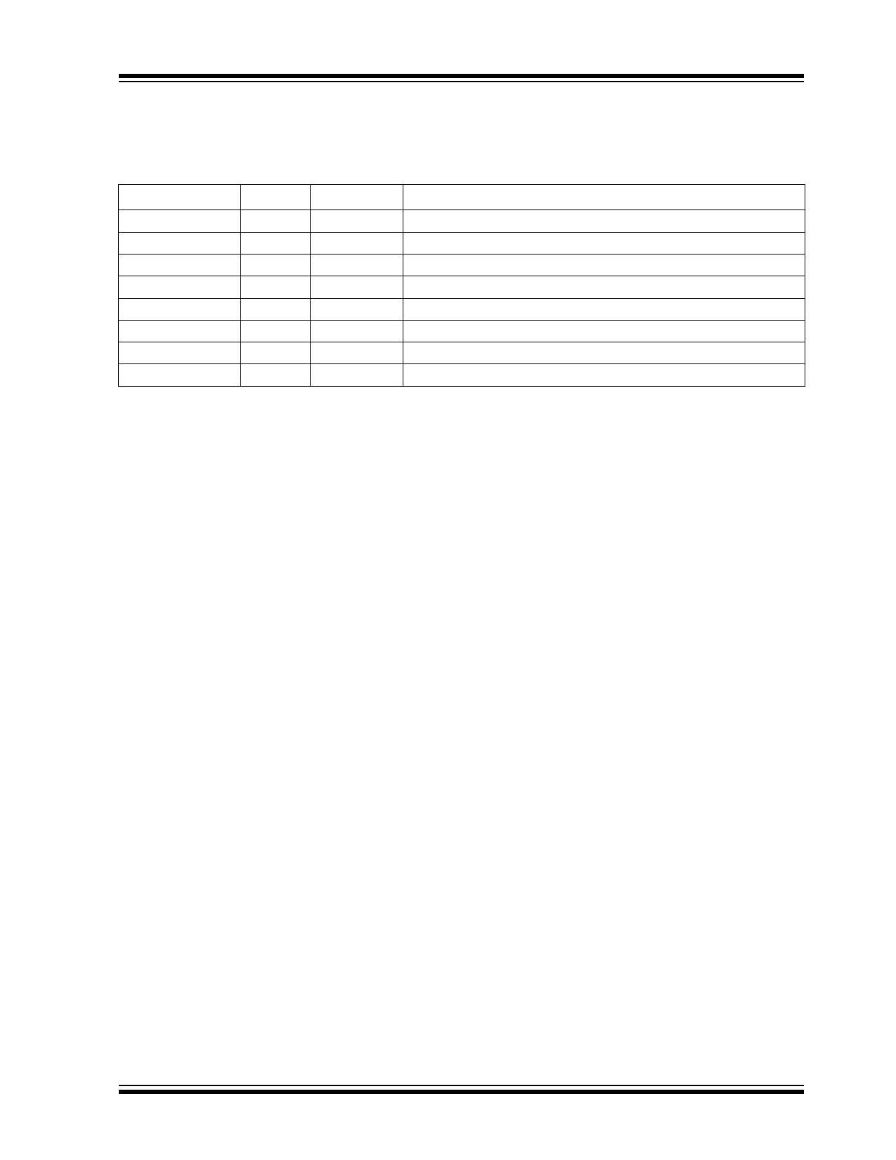
TABLE 2-1: PIN FUNCTION TABLE
Pin Number
Pin Name
Type
1
VREF
Input
2
SDA
Bi-Directional
3
SCL
Input
4
VSS
Power
5
VOUT
Output
6
NC
None
7
DAC-OUT Output
8
VDD
Power
Description
Voltage Reference Input Pin
Serial Data Input/Output Pin
Serial Clock Input Pin
Ground Reference Pin
Buffered Analog Voltage Output Pin
No connection
Unbuffered Analog Voltage Output Pin
Positive Power Supply Input Pin
2.1 External Voltage Reference Input
(VREF)
Voltage Reference Input can range from 0V to 1.2V
below VDD.
2.2 Bi-Directional Serial Data Input
and Output (SDA)
Serial data is transferred on the SMBus in both
directions using this pin.
2.3 Serial Clock Input (SCL)
SMBus/I2C serial clock. Clocks data into and out of the
TC1321.
2.6 No Connection (NC)
There is not a connection at this pin.
2.7 Output (DAC-OUT)
Unbuffered DAC output voltage. This voltage is a
function of the reference voltage and the contents of
the DATA register. This output is unbuffered and care
must be taken that the pin is connected only to a
high-impedance node.
2.8 Positive Power Supply Input (VDD)
See the Electrical Specifications table.
2.4 Supply Power Ground (VSS)
The ground reference pin.
2.5 Output (VOUT)
Buffered DAC output voltage. This voltage is a function
of the reference voltage and the contents of the DATA
register.
2010 Microchip Technology Inc.
DS21387C-page 5
Share Link: 