MT41J128M View Datasheet(PDF) - Micron Technology
Part Name
Description
Manufacturer
MT41J128M Datasheet PDF : 214 Pages
| |||
1Gb: x4, x8, x16 DDR3 SDRAM
Functional Block Diagrams
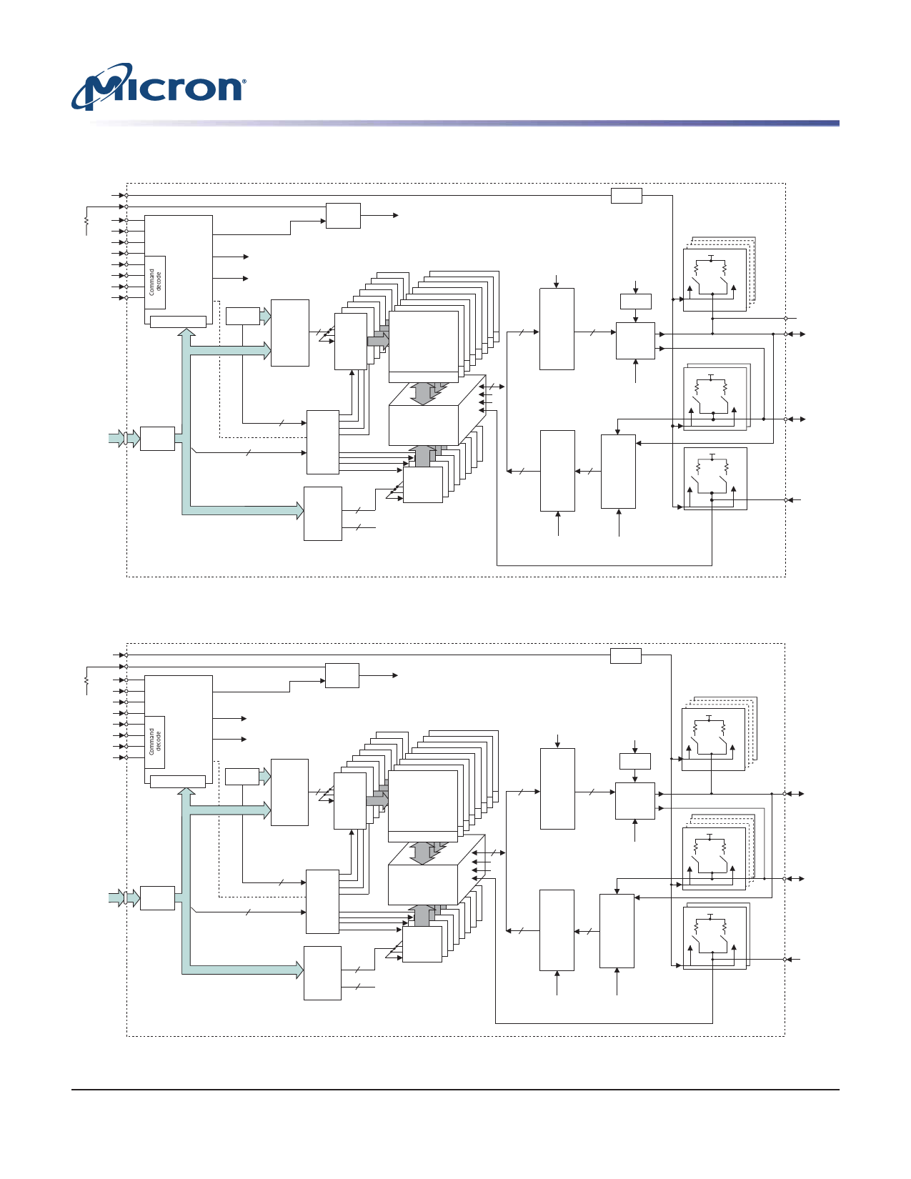
Figure 4: 128 Meg x 8 Functional Block Diagram
ODT
ZQ
RZQ RESET#
CKE
VSSQ A12
CK, CK#
CS#
RAS#
CAS#
WE#
Control
logic
Mode registers
16
A[13:0]
BA[2:0]
17
Address
register
ZQCL, ZQCS
ZQ CAL
To ODT/output drivers
ODT
control
BC4 (burst chop)
OTF
Refresh
counter 14
Row-
14
address
MUX
14
Bank 7
Bank 6
Bank 5
Bank 4
Bank 3
Bank 2
Bank 1
Bank 7
Bank 6
Bank 5
Bank 4
Bank 3
Bank 2
Bank 1
Bank 0
row-
address
latch
and
decoder
16,384
Bank 0
memory
array
(16,384 x 128 x 64)
Sense amplifiers
8,192
3
Bank
control
logic
3
I/O gating
DM mask logic
(128
x64)
Column
decoder
Column-
7
10
address
counter/
latch
3
Columns 0, 1, and 2
Columns 0, 1, and 2
READ
64
FIFO
8
and
data
MUX
64
BC4
OTF
CK, CK#
DLL
READ
drivers
BC4
WRITE
64
Data
8
drivers
interface Data
and
input
logic
CK, CK#
Column 2
(select upper or
lower nibble for BC4)
VDDQ/2
RTT,nom RTT(WR)
sw1
sw2
DQ[7:0]
DQ8
DQS, DQS#
(1 . . . 8)
TDQS#
DQ[7:0]
VDDQ/2
RTT,nom
sw1
RTT(WR)
sw2
(1, 2)
DQS, DQS#
VDDQ/2
RTT,nom RTT(WR)
sw1
sw2
DM/TDQS
(shared pin)
Figure 5: 64 Meg x 16 Functional Block Diagram
ODT
ZQ
RZQ RESET#
CKE
VSSQ A12
CK, CK#
CS#
RAS#
CAS#
WE#
Control
logic
Mode registers
16
A[12:0]
BA[2:0]
16 Address
register
ZQCL, ZQCS
ZQ CAL
To ODT/output drivers
ODT
control
BC4 (burst chop)
OTF
Refresh
counter
13
Row-
13
address
MUX
13
Bank 7
Bank 6
Bank 5
Bank 4
Bank 3
Bank 2
Bank 1
Bank 7
Bank 6
Bank 5
Bank 4
Bank 3
Bank 2
Bank 1
Bank 0
row-
address
latch
and
decoder
8,192
Bank 0
memory
array
(8192 x 128 x 128)
Sense amplifiers
16,384
3
Bank
control
logic
3
I/O gating
DM mask logic
(128
x128)
Column
decoder
Column-
7
10
address
counter/
latch
3
Columns 0, 1, and 2
Column 0, 1, and 2
READ
128
FIFO
16
and
data
MUX
CK, CK#
DLL
READ
drivers
128
BC4
BC4
OTF
128
Data
WRITE
16
drivers
interface
Data
and
input
logic
CK, CK#
Column 2
(select upper or
lower nibble for BC4)
VDDQ/2
RTT,nom RTT(WR)
sw1
sw2
(1 . . . 16)
DQ[15:0]
LDQS, LDQS#, UDQS, UDQS#
DQ[15:0]
VDDQ/2
RTT,nom RTT(WR)
sw1
sw2
(1 . . . 4)
VDDQ/2
RTT,nom RTT(WR)
sw1
sw2
LDQS, LDQS#
UDQS, UDQS#
(1, 2)
LDM/UDM
PDF: 09005aef826aa906
1Gb_DDR3_SDRAM.pdf - Rev. L 03/13 EN
15
Micron Technology, Inc. reserves the right to change products or specifications without notice.
2006 Micron Technology, Inc. All rights reserved.
Share Link: 