S25FL127S View Datasheet(PDF) - Spansion Inc.
Part Name
Description
Manufacturer
S25FL127S Datasheet PDF : 131 Pages
| |||
Data Sheet (Preliminary)
A configuration bit SR2[5] may be set to 1 to replace the HOLD# / IO3 functions with the IO3 / RESET#
functions. Then the IO3 / RESET# may be used to initiate the hardware reset function. The IO3 / RESET#
input is only treated as RESET# when the device is not in Quad-I/O mode, CR1[1] = 0, or when CS# is high.
When Quad I/O mode is in use, CR1[1]=1, and the device is selected with CS# low, the IO3 / RESET# is used
only as IO3 for information transfer. When CS# is high, the IO3 / RESET# is not in use for information transfer
and is used as the RESET# input. By conditioning the reset operation on CS# high during Quad mode, the
reset function remains available during Quad mode.
When the system enters a reset condition, the CS# signal must be driven high as part of the reset process
and the IO3 / RESET# signal is driven low. When CS# goes high the IO3 / RESET# input transitions from
being IO3 to being the RESET# input. The reset condition is then detected when CS# remains high and the
IO3 / RESET# signal remains low for tRP.
The HOLD#/IO3 or IO3/RESET# signals have an internal pull-up resistor and may be left unconnected in the
host system if not used for Quad mode or the reset function.
When Quad mode is enabled, IO3 / RESET# is ignored for tCS following CS# going high. This allows some
time for the memory or host system to actively drive IO3 / RESET# to a valid level following the end of a
transfer. Following the end of a Quad I/O read the memory will actively drive IO3 high before disabling the
output during tDIS. Following a transfer in which IO3 was used to transfer data to the memory, e.g. the QPP
command, the host system is responsible for driving IO3 high before disabling the host IO3 output. This will
ensure that IO3 / Reset is not left floating or being pulled slowly to high by the internal or an external passive
pull-up. Thus, an unintended reset is not triggered by the IO3 / RESET# not being recognized as high before
the end of tRP. Once IO3 / RESET# is high the memory or host system can stop driving the signal. The
integrated pull-up on IO3 will then hold IO3 high unless the host system actively drives IO3 / RESET# to
initiate a reset.
Note that IO3 / Reset# cannot be shared by more than one SPI-MIO memory if any of them are operating in
Quad I/O mode as IO3 being driven to or from one selected memory may look like a reset signal to a second
not selected memory sharing the same IO3 / RESET# signal. See Section 6.3.3, IO3 / RESET# Input Initiated
Hardware (Warm) Reset on page 39 for the IO3 / RESET timing.
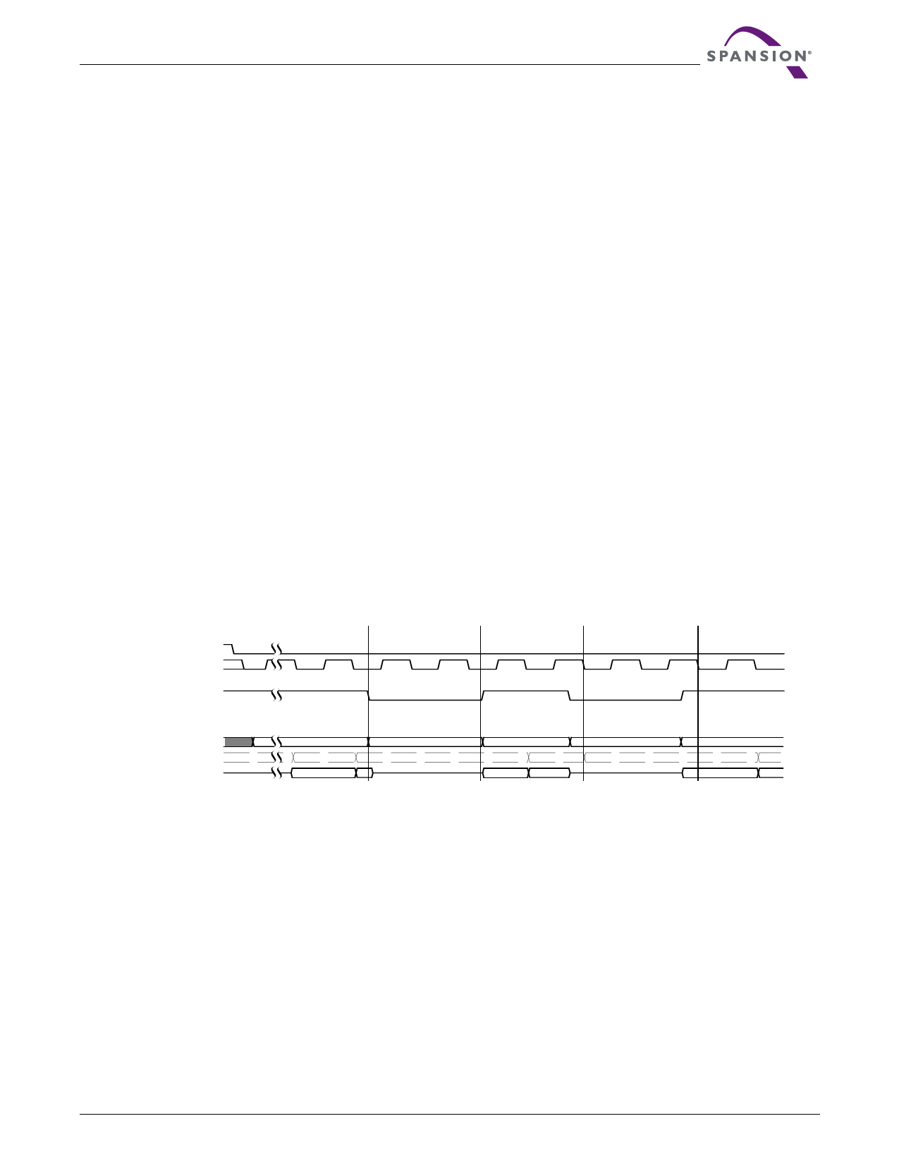
Figure 3.1 HOLD Mode Operation
CS#
SCLK
HOLD#
SI_or_IO_(during_input)
SO_or_IO_(internal)
SO_or_IO_(external)
Valid Input
A
A
Hold Condition
Standard Use
Don't Care
B
B
Valid Input
C
B
C
Hold Condition
Non-standard Use
Don't Care
D
Valid Input
E
D
E
3.10
Voltage Supply (VCC)
VCC is the voltage source for all device internal logic. It is the single voltage used for all device internal
functions including read, program, and erase. The voltage may vary from 2.7V to 3.6V.
3.11
Supply and Signal Ground (VSS)
VSS is the common voltage drain and ground reference for the device core, input signal receivers, and output
drivers.
3.12
Not Connected (NC)
No device internal signal is connected to the package connector nor is there any future plan to use the
connector for a signal. The connection may safely be used for routing space for a signal on a Printed Circuit
Board (PCB). However, any signal connected to an NC must not have voltage levels higher than VCC.
April 25, 2013 S25FL127S_00_02
S25FL127S
19
Share Link: 