SST25VF040B View Datasheet(PDF) - Silicon Storage Technology
Part Name
Description
Manufacturer
SST25VF040B Datasheet PDF : 33 Pages
| |||
Data Sheet
4 Mbit SPI Serial Flash
SST25VF040B
CE#
MODE 3
SCK MODE 0
0 1 2345 6 7
SI
06
MSB
SO
HIGH IMPEDANCE
1295 WREN.0
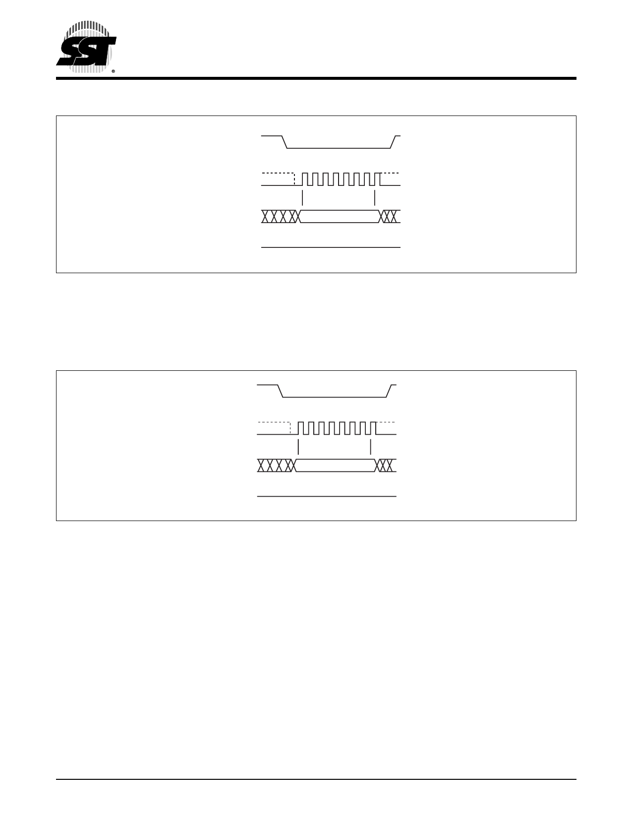
FIGURE 17: Write Enable (WREN) Sequence
Write-Disable (WRDI)
The Write-Disable (WRDI) instruction resets the Write-
Enable-Latch bit and AAI bit to 0 disabling any new Write
operations from occurring. The WRDI instruction will not
terminate any programming operation in progress. Any pro-
gram operation in progress may continue up to TBP after
executing the WRDI instruction. CE# must be driven high
before the WRDI instruction is executed.
CE#
MODE 3
SCK MODE 0
0 1 2345 6 7
SI
04
MSB
SO
HIGH IMPEDANCE
1295 WRDI.0
FIGURE 18: Write Disable (WRDI) Sequence
Enable-Write-Status-Register (EWSR)
The Enable-Write-Status-Register (EWSR) instruction
arms the Write-Status-Register (WRSR) instruction and
opens the status register for alteration. The Write-Status-
Register instruction must be executed immediately after the
execution of the Enable-Write-Status-Register instruction.
This two-step instruction sequence of the EWSR instruc-
tion followed by the WRSR instruction works like SDP (soft-
ware data protection) command structure which prevents
any accidental alteration of the status register values. CE#
must be driven low before the EWSR instruction is entered
and must be driven high before the EWSR instruction is
executed.
©2009 Silicon Storage Technology, Inc.
18
S71295-05-000
10/09
Share Link: 