UPD17217CT-XXX View Datasheet(PDF) - NEC => Renesas Technology
Part Name
Description
Manufacturer
UPD17217CT-XXX
NEC => Renesas Technology

UPD17217CT-XXX Datasheet PDF : 84 Pages
| |||
µPD17215, 17216, 17217, 17218
(5) General-purpose data memory
The general-purpose data memory area is an area of the data memory excluding the system register area,
and the port register area. This memory area has a total of 223 nibbles (111 nibbles in BANK0 and 112 nibbles
in BANK1).
µPD17215 and 17216 are not provided with BANK1.
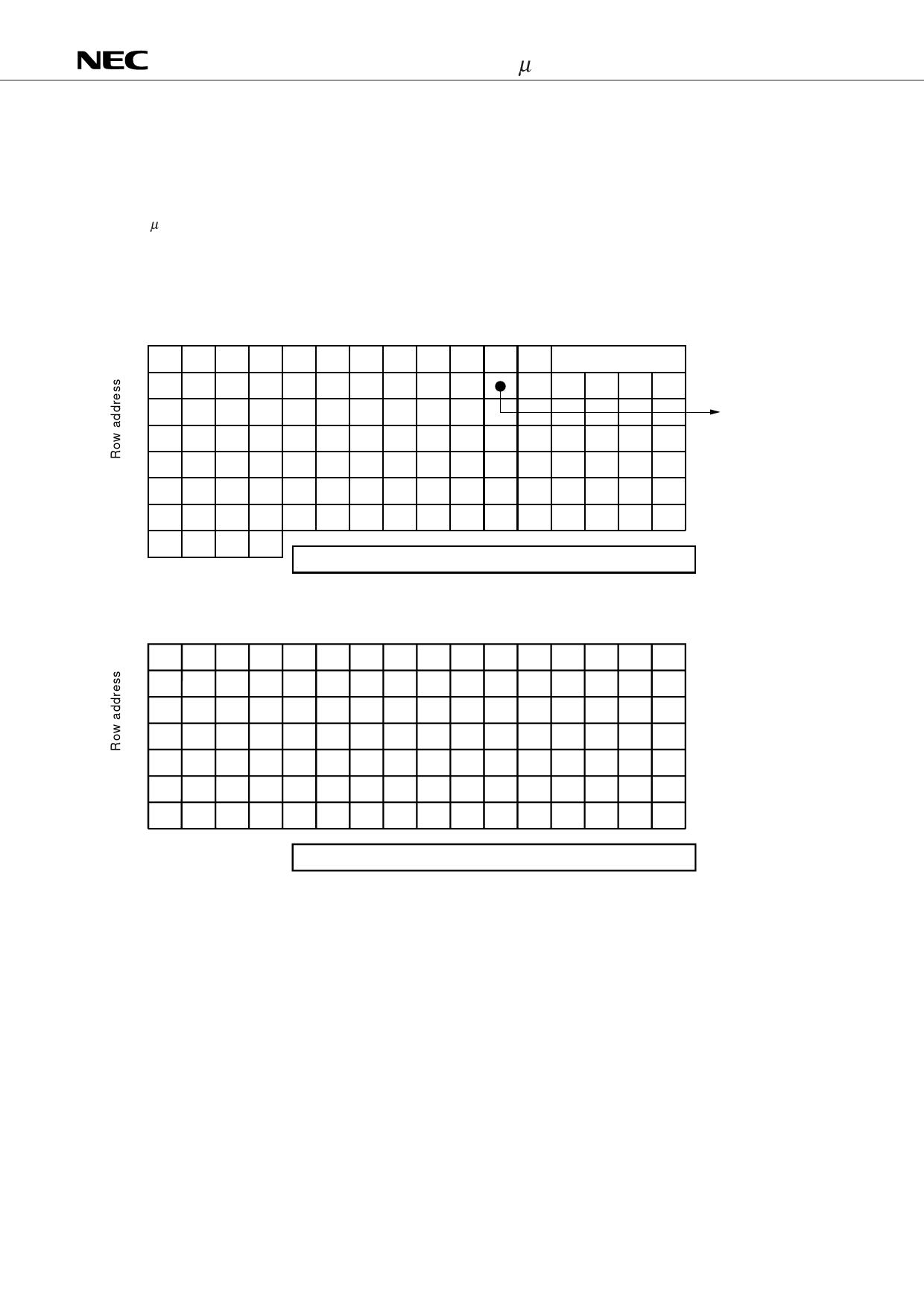
Fig. 2-4 Configuration of Data Memory
Column address
BANK 0
0 1 2 3 4 5 6 7 8 9 ABCDEF
0
Data buffer (DBF)
1
2
3
4
5
6
P0E
7 P0A P0B P0C P0D
System register (SYSREG)
Example:
Address 1AH
in BANK 0
Column address
BANK 1
0 1 2 3 4 5 6 7 8 9 ABCDEF
System register (SYSREG)
Caution:
No data can be written to the addresses 70H to 73H of BANK1 (the value of P0A to P0D are read
in this case).
15
Share Link: