SST25VF016B View Datasheet(PDF) - Microchip Technology
Part Name
Description
Manufacturer
SST25VF016B Datasheet PDF : 30 Pages
| |||
SST25VF016B
5.0 ELECTRICAL SPECIFICATIONS
Absolute Maximum Stress Ratings (Applied conditions greater than those listed under “Absolute Maxi-
mum Stress Ratings” may cause permanent damage to the device. This is a stress rating only and func-
tional operation of the device at these conditions or conditions greater than those defined in the operational
sections of this data sheet is not implied. Exposure to absolute maximum stress rating conditions may
affect device reliability.)
Temperature Under Bias . . . . . . . . . . . . . . . . . . . . . . . . . . . . . . . . . . . . . . . . . . . . . . . . . -55°C to +125°C
Storage Temperature . . . . . . . . . . . . . . . . . . . . . . . . . . . . . . . . . . . . . . . . . . . . . . . . . . . . -65°C to +150°C
D. C. Voltage on Any Pin to Ground Potential . . . . . . . . . . . . . . . . . . . . . . . . . . . . . . . .-0.5V to VDD+0.5V
Transient Voltage (<20 ns) on Any Pin to Ground Potential . . . . . . . . . . . . . . . . . . . . . .-2.0V to VDD+2.0V
Package Power Dissipation Capability (TA = 25°C) . . . . . . . . . . . . . . . . . . . . . . . . . . . . . . . . . . . . . . 1.0W
Surface Mount Solder Reflow Temperature . . . . . . . . . . . . . . . . . . . . . . . . . . . . . . . 260°C for 10 seconds
Output Short Circuit Current1 . . . . . . . . . . . . . . . . . . . . . . . . . . . . . . . . . . . . . . . . . . . . . . . . . . . . . . 50 mA
1. Output shorted for no more than one second. No more than one output shorted at a time.
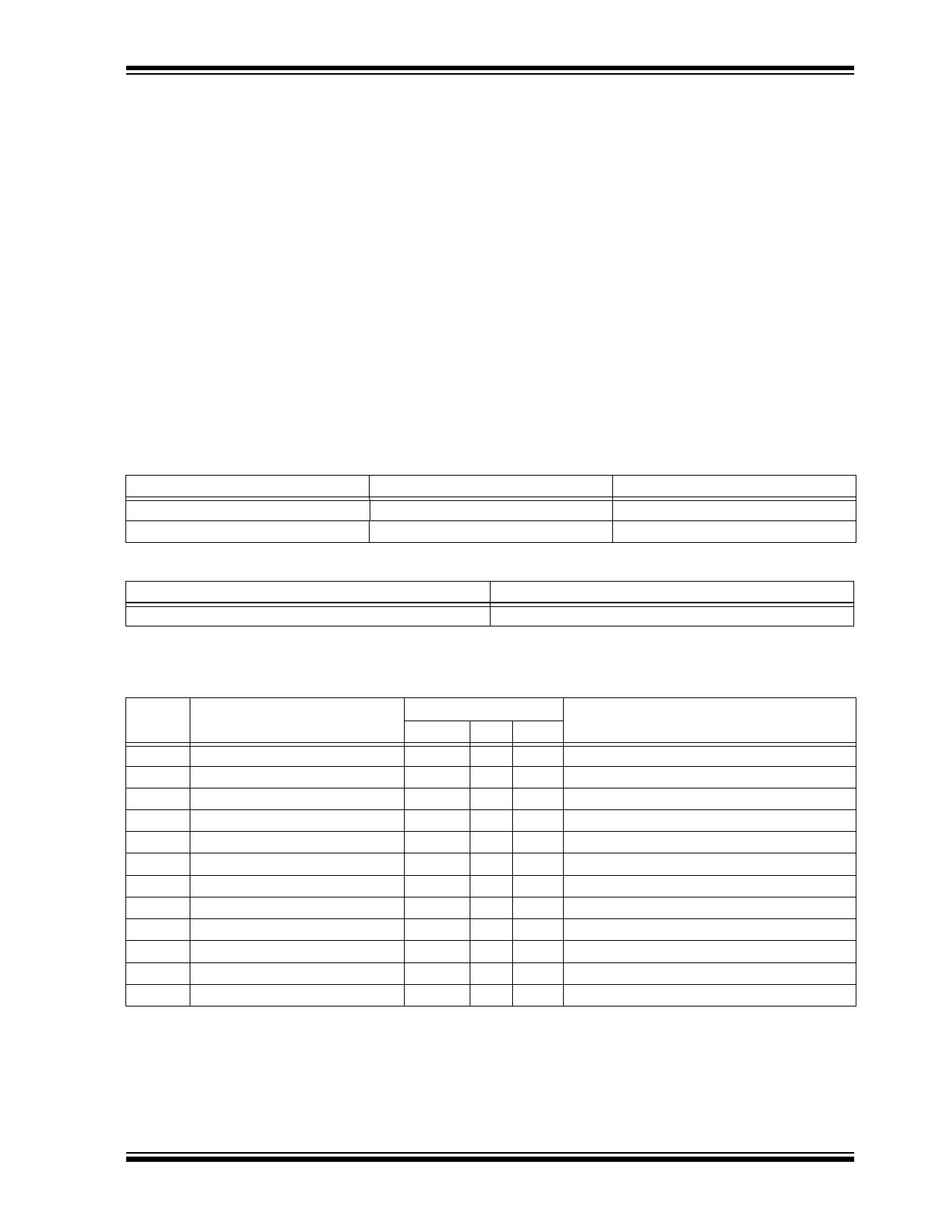
TABLE 5-1:
Range
Commercial
Industrial
OPERATING RANGE
Ambient Temp
0°C to +70°C
-40°C to +85°C
TABLE 5-2:
AC CONDITIONS OF TEST1
Input Rise/Fall Time
5ns
1. See Figures 5-5 and 5-6
VDD
2.7-3.6V
2.7-3.6V
Output Load
CL = 30 pF
TABLE 5-3: DC OPERATING CHARACTERISTICS
Limits
Symbol Parameter
IDDR
IDDR2
IDDR3
IDDW
ISB
ILI
ILO
VIL
VIH
VOL
VOL2
VOH
Read Current
Read Current
Read Current
Program and Erase Current
Standby Current
Input Leakage Current
Output Leakage Current
Input Low Voltage
Input High Voltage
Output Low Voltage
Output Low Voltage
Output High Voltage
Min
0.7 VDD
VDD-0.2
Max
10
15
20
30
20
1
1
0.8
0.2
0.4
Units
mA
mA
mA
mA
µA
µA
µA
V
V
V
V
V
Test Conditions
CE#=0.1 VDD/0.9 VDD@25 MHz, SO=open
CE#=0.1 VDD/0.9 VDD@50 MHz, SO=open
CE#=0.1 VDD/0.9 VDD@50 MHz, SO=open
CE#=VDD
CE#=VDD, VIN=VDD or VSS
VIN=GND to VDD, VDD=VDD Max
VOUT=GND to VDD, VDD=VDD Max
VDD=VDD Min
VDD=VDD Max
IOL=100 µA, VDD=VDD Min
IOL=1.6 mA, VDD=VDD Min
IOH=-100 µA, VDD=VDD Min
2015 Microchip Technology Inc.
Downloaded from: http://www.datasheetcatalog.com/
DS20005044C-page 19
Share Link: 