AT89C5131A-M(2005) View Datasheet(PDF) - Atmel Corporation
Part Name
Description
Manufacturer
AT89C5131A-M Datasheet PDF : 184 Pages
| |||
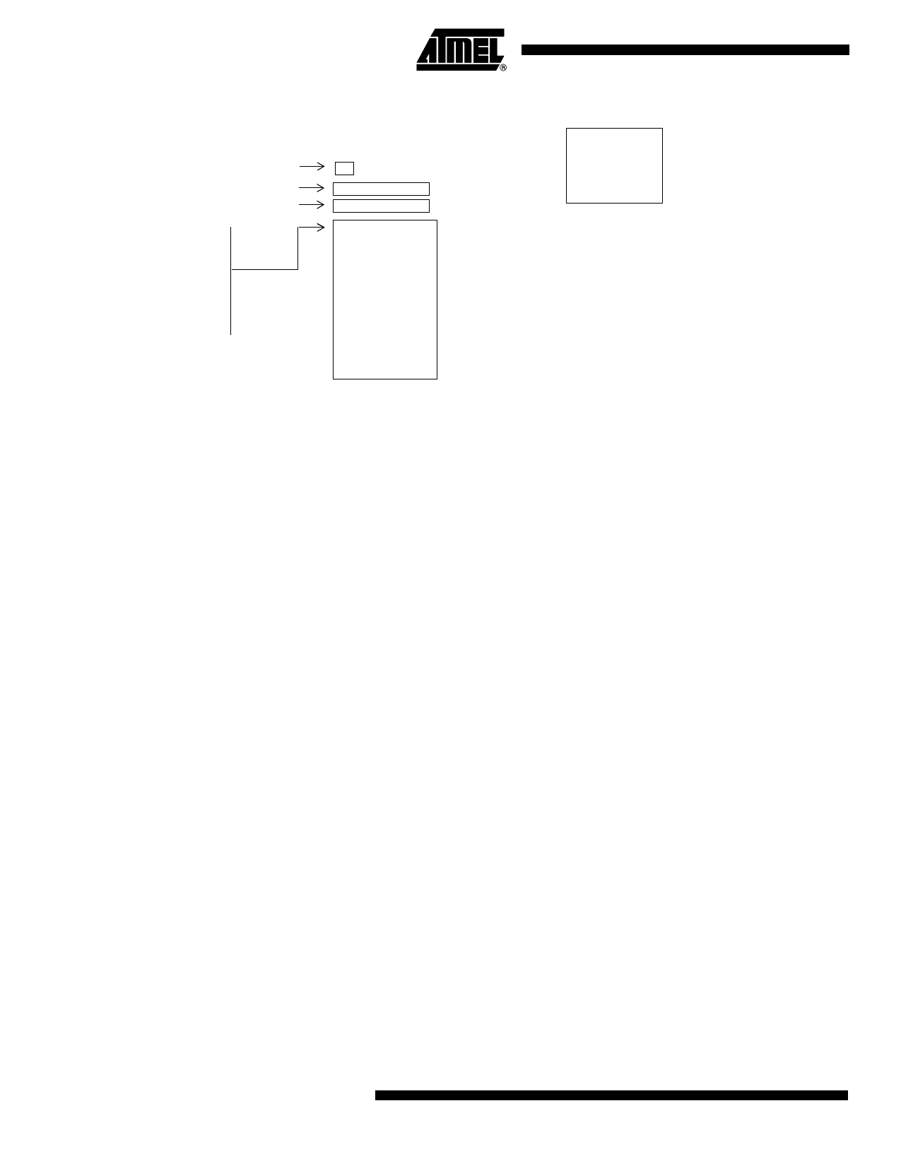
Figure 14. Flash Memory Architecture
Hardware Security (1 Byte)
Extra Row (128 Bytes)
Column Latches (128 Bytes)
3FFFh for
AT89C5130A
for 16 KB
7FFFh for
AT89C5131A
for 32 KB
16/32 KB
Flash Memory
User Space
FM0
3 Kbytes
Flash Memory
Boot Space
FM1
FFFFh
F400h
FM1 mapped between FFFFh and
F400h when bit ENBOOT is set in
AUXR1 register
0000h
FM0 Memory Architecture
The Flash memory is made up of 4 blocks (see Figure 14):
1. The memory array (user space) 32 Kbytes
2. The Extra Row
3. The Hardware security bits
4. The column latch registers
User Space
This space is composed of a 16/32 Kbytes Flash memory organized in 128/256 pages
of 128 bytes. It contains the user’s application code.
Extra Row (XRow)
This row is a part of FM0 and has a size of 128 bytes. The extra row may contain infor-
mation for bootloader usage.
Hardware Security Space
The hardware security space is a part of FM0 and has a size of 1 byte.
The 4 MSB can be read/written by software. The 4 LSB can only be read by software
and written by hardware in parallel mode.
Column Latches
The column latches, also part of FM0, have a size of full page (128 bytes).
The column latches are the entrance buffers of the three previous memory locations
(user array, XRow and Hardware security byte).
Overview of FM0
Operations
The CPU interfaces to the Flash memory through the FCON register and AUXR1
register.
These registers are used to:
• Map the memory spaces in the adressable space
• Launch the programming of the memory spaces
• Get the status of the Flash memory (busy/not busy)
• Select the Flash memory FM0/FM1.
Mapping of the Memory Space
By default, the user space is accessed by MOVC instruction for read only. The column
latches space is made accessible by setting the FPS bit in FCON register. Writing is
possible from 0000h to 3FFFH/7FFFh, address bits 6 to 0 are used to select an address
within a page while bits 14 to 7 are used to select the programming address of the page.
Setting this bit takes precedence on the EXTRAM bit in AUXR register.
30 AT89C5130A/31A-M
4337C–USB–02/05
Share Link: 