IS43TR16640A-125KBL View Datasheet(PDF) - Unspecified
Part Name
Description
Manufacturer
IS43TR16640A-125KBL Datasheet PDF : 71 Pages
| |||
IS43TR16640A, IS43TR81280A
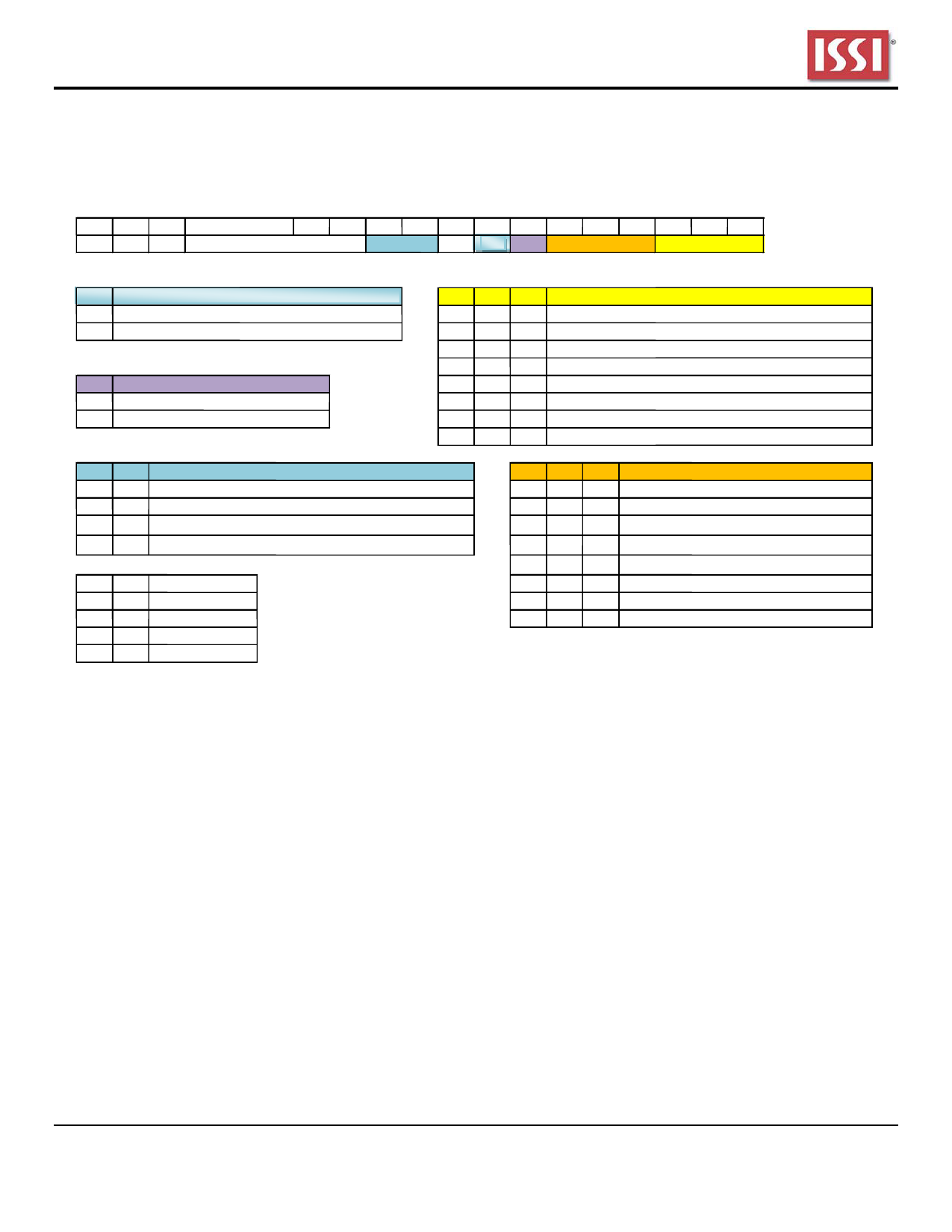
2.3.4 Mode Register MR2
The Mode Register MR2 stores the data for controlling refresh related features, Rtt_WR impedance, and CAS write
latency. The Mode Register 2 is written by asserting low on CS#, RAS#, CAS#, WE#, high on BA1 and low on BA0 and
BA2, while controlling the states of address pins according to the below.
BA2 BA1 BA0
010
A13
A12 A11 A10 A9 A8 A7 A6 A5 A4 A3 A2 A1 A0 Address Field
0* 1
Rtt_WR 0* 1 SRT ASR
CWL
PASR
Mode Register 2
A7
Self-Refresh Temperature (SRT) Range
0
Normal operating temperature range
1
Extended operating temperature range
A6
Auto Self-Refresh (ASR)
0
Manual SR Reference (SRT)
1
ASR enable
A2 A1 A0
000
001
010
011
100
101
110
111
Partial Array Self-Refresh (Optional)
Full Array
HalfArray (BA[2:0]=000,001,010, &011)
Quarter Array (BA[2:0]=000, & 001)
1/8th Array (BA[2:0] = 000)
3/4 Array (BA[2:0] = 010,011,100,101,110, & 111)
HalfArray (BA[2:0] = 100, 101, 110, &111)
Quarter Array (BA[2:0]=110, &111)
1/8th Array (BA[2:0]=111)
A10 A9
00
01
10
11
BA1 BA0
00
01
10
11
Rtt_WR *2
Dynamic ODT off (Write does not affect Rtt value)
RZQ/4
RZQ/2
Reserved
MR Select
MR0
MR1
MR2
MR3
A5 A4 A3
000
001
010
011
100
101
110
111
CAS write Latency (CWL)
5 (tCK(avg) 2.5 ns)
6 (2.5 ns > tCK(avg) 1.875 ns)
7 (1.875 ns > tCK(avg) 1.5 ns)
8 (1.5 ns > tCK(avg) 1.25 ns)
9 (1.25 ns > tCK(avg) 1.07ns)
10 (1.07 ns > tCK(avg) 0.935 ns)
11 (0.935 ns > tCK(avg) 0.833 ns)
12 (0.833 ns > tCK(avg) 0.75 ns)
* 1 : A5, A8, A11 ~ A13 must be programmed to 0 during MRS.
* 2 : The Rtt_WR value can be applied during writes even when Rtt_Nom is disabled. During write leveling, Dynamic ODT is not available.
Figure 2.3.4 MR2 Definition
2.3.4.1 Partial Array Self-Refresh (PASR)
If PASR (Partial Array Self-Refresh) is enabled, data located in areas of the array beyond the specified address range
shown in Figure 2.3.4 will be lost if Self-Refresh is entered. Data integrity will be maintained if tREFI conditions are met
and no Self-Refresh command is issued.
2.3.4.2 CAS Write Latency (CWL)
The CAS Write Latency is defined by MR2 (bits A3-A5), as shown in Figure 2.3.4. CAS Write Latency is the delay, in clock
cycles, between the internal Write command and the availability of the first bit of input data. DDR3 SDRAM does not
support any half-clock latencies. The overall Write Latency (WL) is defined as Additive Latency (AL) + CAS Write Latency
(CWL); WL = AL + CWL. For more information on the supported CWL and AL settings based on the operating clock
frequency, refer to “Standard Speed Bins”.
2.3.4.3 Auto Self-Refresh (ASR) and Self-Refresh Temperature (SRT)
For more details refer to “Extended Temperature Usage”. DDR3 SDRAMs support Self-Refresh operation at all supported
temperatures. Applications requiring Self-Refresh operation in the Extended Temperature Range must use the ASR
function or program the SRT bit appropriately.
Integrated Silicon Solution, Inc. – www.issi.com –
14
Rev. 00A
04/16/2012
Share Link: 