IS43TR16640A-125KBL View Datasheet(PDF) - Unspecified
Part Name
Description
Manufacturer
IS43TR16640A-125KBL Datasheet PDF : 71 Pages
| |||
IS43TR16640A, IS43TR81280A
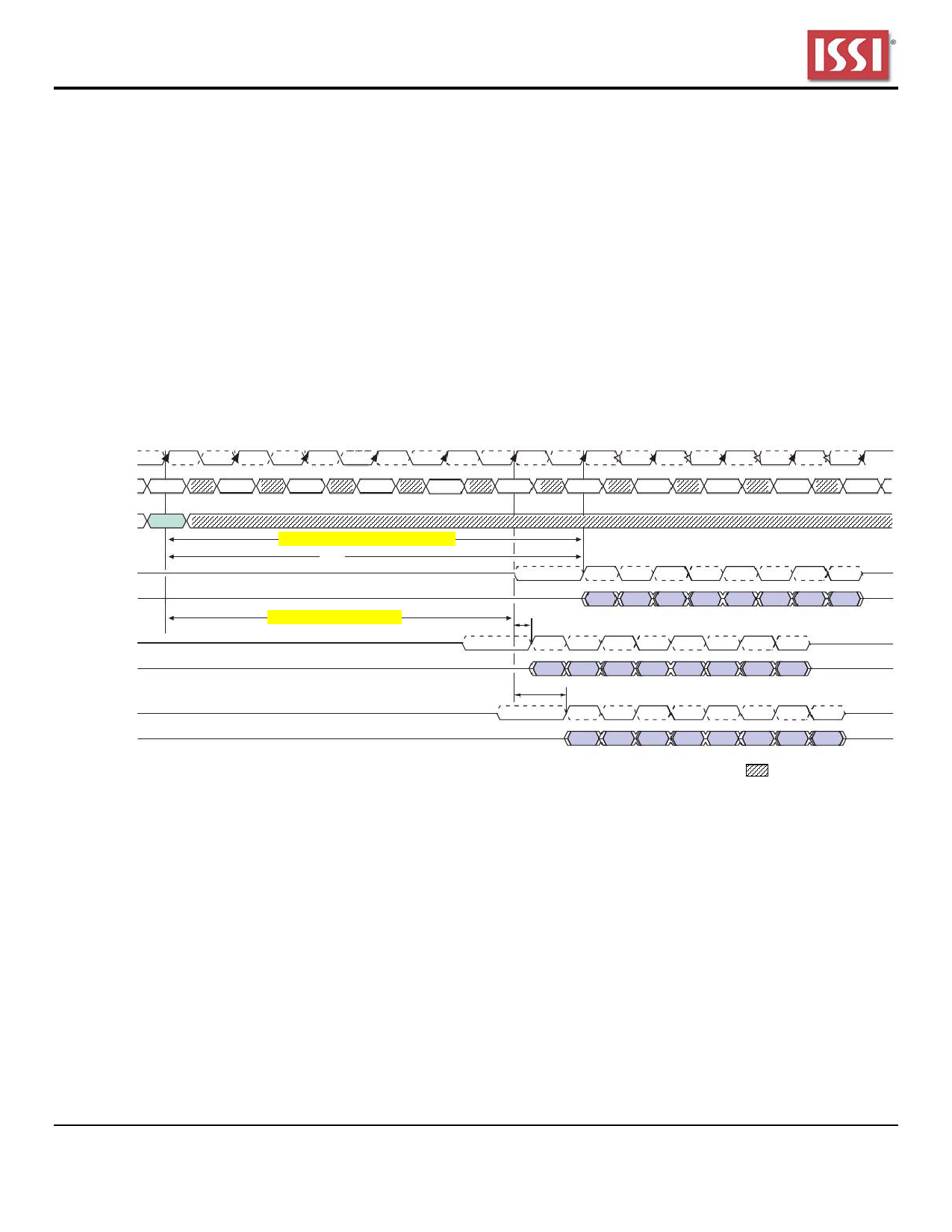
2.4.4 DLL-off Mode
DDR3 DLL-off mode is entered by setting MR1 bit A0 to “1”; this will disable the DLL for subsequent operations until A0 bit
set back to “0”. The MR1 A0 bit for DLL control can be switched either during initialization or later. The DLL-off Mode
operations listed below are an optional feature for DDR3. The maximum clock frequency for DLL-off Mode is specified by
the parameter tCKDLL_OFF. There is no minimum frequency limit besides the need to satisfy the refresh interval, tREFI.
Due to latency counter and timing restrictions, only one value of CAS Latency (CL) in MR0 and CAS Write Latency (CWL)
in MR2 are supported. The DLL-off mode is only required to support setting of both CL=6 and CWL=6. DLL-off mode will
affect the Read data Clock to Data Strobe relationship (tDQSCK) but not the data Strobe to Data relationship (tDQSQ,
tQH). Special attention is needed to line up Read data to controller time domain.
Comparing with DLL-on mode, where tDQSCK starts from the rising clock edge (AL+CL) cycles after the Read command,
the DLL-off mode tDQSCK starts (AL+CL-1) cycles after the read command. Another difference is that tDQSCK may not
be small compared to tCK (it might even be larger than tCK) and the difference between tDQSCKmin and tDQSCKmax is
significantly larger than in DLL-on mode. The timing relations on DLL-off mode READ operation have shown at the
following Timing Diagram (CL=6, BL=8)
T0
T1
T2
T3
T4
T5
T6
T7
T8
T9
T10
CK#
CK
Command
READ
NOP
NOP
NOP
NOP
NOP
NOP
NOP
NOP
NOP
NOP
Address
DQS,DQS#(DLL_on)
RL (DLL_on) = AL+CL =6 (CL=6,AL=0)
CL=6
DQ(DLL_on)
DQS,DQS#(DLL_off)
RL (DLL_off) = AL+(CL-1) = 5
tDQSCK(DLL_off)_min
DQ(DLL_off)
DQS,DQS#(DLL_off)
tDQSCK(DLL_off)_max
DQ(DLL_off)
Don’t Care
Note: The tDQSCK is used here for DQS, DQS, and DQ to have a simplified diagram; the DLL_off shift will affect both timings in the same way and the
skew between all DQ, DQS, and DQS# signals will still be tDQSQ.
Figure 2.4.4 DLL-off mode READ Timing Operation
Integrated Silicon Solution, Inc. – www.issi.com –
21
Rev. 00A
04/16/2012
Share Link: 