SST25VF032B View Datasheet(PDF) - Silicon Storage Technology
Part Name
Description
Manufacturer
SST25VF032B Datasheet PDF : 28 Pages
| |||
32 Mbit SPI Serial Flash
SST25VF032B
Auto Address Increment (AAI) Word-Program
The AAI program instruction allows multiple bytes of data to
be programmed without re-issuing the next sequential
address location. This feature decreases total program-
ming time when multiple bytes or entire memory array is to
be programmed. An AAI Word program instruction pointing
to a protected memory area will be ignored. The selected
address range must be in the erased state (FFH) when ini-
tiating an AAI Word Program operation. While within AAI
Word Programming sequence, the only valid instructions
are AAI Word (ADH), RDSR (05H), or WRDI (04H). Users
have three options to determine the completion of each
AAI Word program cycle: hardware detection by reading
the Serial Output, software detection by polling the BUSY
bit in the software status register or wait TBP. Refer to End-
Of-Write Detection section for details.
Prior to any write operation, the Write-Enable (WREN)
instruction must be executed. The AAI Word Program
instruction is initiated by executing an 8-bit command,
ADH, followed by address bits [A23-A0]. Following the
addresses, two bytes of data is input sequentially, each one
from MSB (Bit 7) to LSB (Bit 0). The first byte of data (D0)
will be programmed into the initial address [A23-A1] with A0
= 0, the second byte of Data (D1) will be programmed into
the initial address [A23-A1] with A0 = 1. CE# must be driven
high before the AAI Word Program instruction is executed.
The user must check the BUSY status before entering the
next valid command. Once the device indicates it is no
longer busy, data for the next two sequential addresses
may be programmed and so on. When the last desired
byte had been entered, check the busy status using the
hardware method or the RDSR instruction and execute the
Write-Disable (WRDI) instruction, 04H, to terminate AAI.
Check the busy status after WRDI to determine if the
device is ready for any command. See Figures 10 and 11
for AAI Word programming sequence.
There is no wrap mode during AAI programming; once the
highest unprotected memory address is reached, the
device will exit AAI operation and reset the Write-Enable-
Latch bit (WEL = 0) and the AAI bit (AAI = 0).
End-of-Write Detection
There are three methods to determine completion of a pro-
gram cycle during AAI Word programming: hardware
detection by reading the Serial Output, software detection
by polling the BUSY bit in the Software Status Register or
wait TBP. The hardware end-of-write detection method is
described in the section below.
Data Sheet
Hardware End-of-Write Detection
The hardware end-of-write detection method eliminates the
overhead of polling the Busy bit in the Software Status
Register during an AAI Word program operation. The 8-bit
command, 70H, configures the Serial Output (SO) pin to
indicate Flash Busy status during AAI Word programming,
as shown in Figure 8. The 8-bit command, 70H, must be
executed prior to executing an AAI Word-Program instruc-
tion. Once an internal programming operation begins,
asserting CE# will immediately drive the status of the inter-
nal flash status on the SO pin. A ‘0’ indicates the device is
busy and a ‘1’ indicates the device is ready for the next
instruction. De-asserting CE# will return the SO pin to tri-
state.
The 8-bit command, 80H, prevents the Serial Output (SO)
pin from outputting Busy status during AAI-Word-program
operation and re-configures SO as an output pin. The
device can only accept the 80H command when the device
is not in AAI mode. Once SO is an output pin, in AAI mode
the device can accept both RDSR instruction for polling
and Software Status Register data outputs through the SO
pin. This is shown in Figure 9.
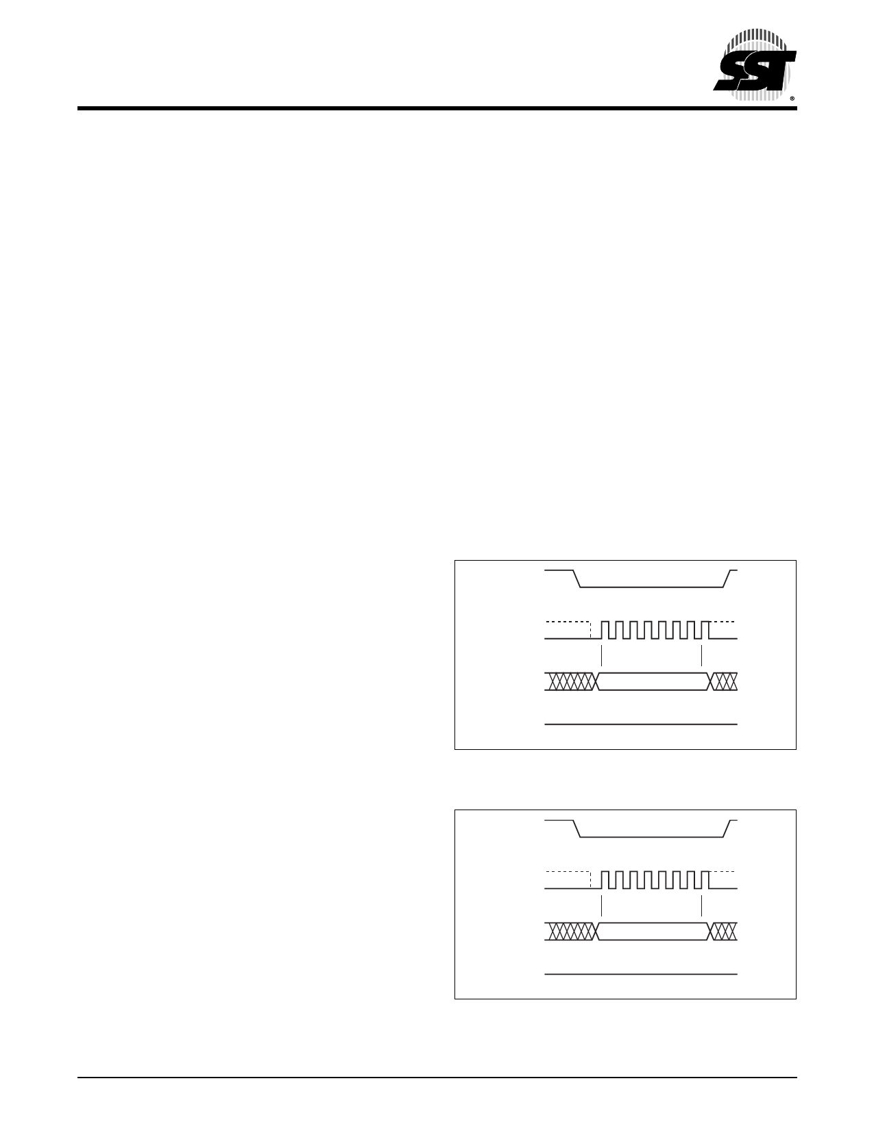
CE#
MODE 3
SCK MODE 0
0 1 2345 6 7
SI
70
MSB
SO
HIGH IMPEDANCE
1327 F09.0
FIGURE 8: Enable SO as Hardware RY/BY#
during AAI Programming
CE#
MODE 3
SCK MODE 0
0 1 2345 6 7
SI
80
MSB
SO
HIGH IMPEDANCE
1327 F10.0
FIGURE 9: Disable SO as Hardware RY/BY#
during AAI Programming
©2009 Silicon Storage Technology, Inc.
11
S71327-03-000
05/09
Share Link: 